Használati útmutató Microchip PIC32MM0064GPM028
Microchip
nincs kategorizálva
PIC32MM0064GPM028
Olvassa el alább 📖 a magyar nyelvű használati útmutatót Microchip PIC32MM0064GPM028 (158 oldal) a nincs kategorizálva kategóriában. Ezt az útmutatót 4 ember találta hasznosnak és 2 felhasználó értékelte átlagosan 4.5 csillagra
Oldal 1/158

© 2013-2015 Microchip Technology Inc. DS60001192B-page 50-1
Section 50. CPU for Devices with MIPS32
®
microAptiv™
and M-Class Cores
This section of the manual contains the following topics:
50.1 Introduction .............................................................................................................. 50-2
50.2 Architecture Overview ............................................................................................. 50-4
50.3 PIC32 CPU Details .................................................................................................. 50-8
50.4 Special Considerations When Writing to CP0 Registers ....................................... 50-13
50.5 MIPS32 Architecture.............................................................................................. 50-14
50.6 CPU Bus................................................................................................................ 50-15
50.7 Internal System Busses......................................................................................... 50-15
50.8 Set/Clear/Invert...................................................................................................... 50-16
50.9 ALU Status Bits...................................................................................................... 50-16
50.10 Interrupt and Exception Mechanism ...................................................................... 50-17
50.11 Programming Model .............................................................................................. 50-17
50.12 Floating Point Unit (FPU)....................................................................................... 50-24
50.13 Coprocessor 0 (CP0) Registers............................................................................. 50-42
50.14 Coprocessor 1 (CP1) Registers........................................................................... 50-121
50.15 microMIPS Execution .......................................................................................... 50-132
50.16 MCU ASE Extension ........................................................................................... 50-132
50.17 MIPS DSP ASE Extension .................................................................................. 50-133
50.18 Memory Model (MCU only).................................................................................. 50-133
50.19 Memory Management (MPU only)....................................................................... 50-135
50.20 L1 Caches (MPU only) ........................................................................................ 50-141
50.21 CPU Instructions.................................................................................................. 50-145
50.22 MIPS DSP ASE Instructions ................................................................................ 50-151
50.23 CPU Initialization ................................................................................................. 50-153
50.24 Effects of a Reset ................................................................................................ 50-154
50.25 Related Application Notes ...................................................................................50-155
50.26 Revision History................................................................................................... 50-156

PIC32 Family Reference Manual
DS60001192B-page 50-2 © 2013-2015 Microchip Technology Inc.
50.1 INTRODUCTION
Depending on the device family, PIC32 devices are a complex System-on-Chip (SoC), which are
based on the microAptiv™ Microprocessor core or the M-Class Microprocessor core from
Imagination Technologies Ltd. This document provides an overview of the CPU system
architecture and features of PIC32 microcontrollers that feature these microprocessor cores.
The microAptiv Microprocessor core is a superset of the MIPS
®
M14KE™ and M14KEc™
Microprocessor cores. These cores are state of the art, 32-bit, low-power, RISC processor cores
with the enhanced MIPS32
®
Release 2 Instruction Set Architecture (ISA).
The M-Class Microprocessor core is a superset of the microAptiv™ Microprocessor core. This
32-bit, low-power, RISC processor core uses the enhanced MIPS32
®
Release 5 Instruction Set
Architecture (ISA).
Visit the Imagination Technologies Ltd. website (www.imgtec.com) to learn more about the
microprocessor cores.
Depending on the core configuration, one of two options, MCU or MPU, are used, as shown in
Table 50-1.
Table 50-1: microAptiv and M-Class Microprocessor Core Configurations
The primary difference between the MCU and MPU is the presence of an L1 cache and
TLB-based MMU on the MPU. These features are used to facilitate PIC32 designs that use
operating systems to manage virtual memory.
Note: This family reference manual section is meant to serve as a complement to device
data sheets. Depending on the device variant, this manual section may not apply to
all PIC32 devices.
Please consult the note at the beginning of the “CPU” chapter in the current device
data sheet to check whether this document supports the device you are using.
Device data sheets and family reference manual sections are available for
download from the Microchip Worldwide Web site at: http://www.microchip.com
MCU Features MPU Features
Split-bus architecture Unified bus architecture
Integrated DSP ASE (see Note 1) Integrated DSP ASE (see Note 1)
Integrated MCU™ ASE Integrated MCU ASE
microMIPS™ code compression microMIPS code compression
FMT-based MMU TLB-based MMU
Two shadow register sets Eight shadow register sets
EJTAG TAP controller EJTAG TAP controller
Performance counters Performance counters
Hardware Trace (iFlowtrace
®
) Hardware Trace (iFlowtrace)
Level One (L1) CPU cache
Note 1: This feature is not available on all devices, refer to the “CPU” chapter of the spe-
cific device data sheet to determine availability.

© 2013-2015 Microchip Technology Inc. DS60001192B-page 50-3
Section 50. CPU for Devices with MIPS32
®
microAptiv™ and M-Class Cores
50.1.1 Key Features Common to All PIC32 Devices with the microAptiv
Microprocessor Core
The following key features are common to all PIC32 devices that are based on the microAptiv
Microprocessor core:
• microMIPS variable-length instruction mode for compact code
• Vectored interrupt controller with up to 256 interrupt sources
• Atomic bit manipulations on peripheral registers (Single cycle)
• High-speed Microchip ICD port with hardware-based non-intrusive data monitoring and
application data streaming functions
• EJTAG debug port allows extensive third party debug, programming and test tools support
• Instruction controlled power management modes
• Five-stage pipelined instruction execution
• Internal code protection to help protect intellectual property
• Arithmetic saturation and overflow handling support
• Zero cycle overhead saturation and rounding operations
• Atomic read-modify-write memory-to-memory instructions
• MAC instructions with up to 4 accumulators
• Native fractional data type (Q15, Q31) with rounding support
• Digital Signal Processing (DSP) Application-Specific Extension (ASE) Revision 2, which adds
DSP capabilities with support for powerful data processing operations
• Multiply/Divide unit with a maximum issue rate of one 32 x 32 multiply per clock
50.1.2 Key Features Common to All PIC32 Devices with the M-Class
Microprocessor Core
In addition to the features described for devices with the microAptiv core, the following key
features are common to all PIC32 devices that are based on the M-Class Microprocessor core:
• Implements the latest MIPS Release 5 Architecture, which includes IP protection and
reliability for industrial controllers, Internet of Things (IoT), wearables, wireless
communications, automotive, and storage
• Floating Point Unit (FPU)
50.1.3 Related MIPS Documentation
Related MIPS documentation is available for download from the related Imagination
Technologies Ltd. product page. Please note that a login may be required to access these
documents.
Documentation for the microAptiv core is available for download at:
http://www.imgtec.com/mips/aptiv/microaptiv.asp
Documentation for the M-Class core is available for download at:
http://www.imgtec.com/mips/warrior/mclass.asp
PIC32 Family Reference Manual
DS60001192B-page 50-4 © 2013-2015 Microchip Technology Inc.
50.2 ARCHITECTURE OVERVIEW
The PIC32 family of devices are complex systems-on-a-chip that contain many features.
Included in all processors of the PIC32 family is a high-performance RISC CPU, which can be
programmed in 32-bit and 16-bit modes, and even mixed modes.
Devices with the M-Class core include a Floating Point Unit (FPU) that implements the MIPS
Release 5 Instruction Set Architecture for floating point computation. The FPU implementation
supports the ANSI/IEEE Standard 754 (IEEE Standard for Binary Floating-Point Arithmetic) for
single- and double-precision data formats.
PIC32 devices contain a high-performance Interrupt Controller, DMA controller, USB controller,
in-circuit debugger, a high-performance switching matrix for high-speed data accesses to the
peripherals, and on-chip data RAM memory, which holds data and programs. The optional
prefetch cache and prefetch buffer for the Flash memory, which hides the latency of the Flash,
provides zero Wait state equivalent performance.
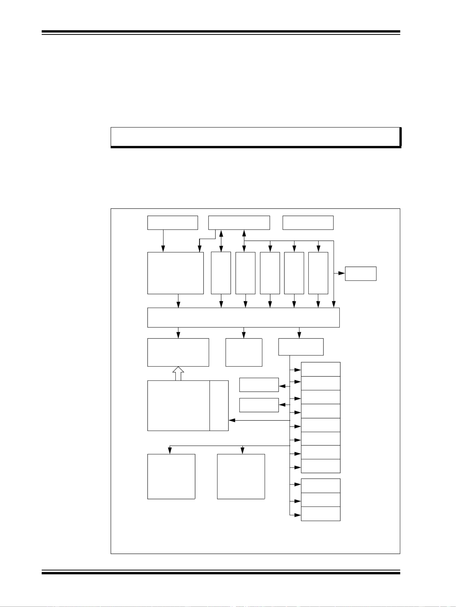
Figure 50-1: PIC32 Block Diagram
Note: Refer to the “CPU” chapter in the specific device data sheet to determine
availability of the FPU module in your device.
JTAG/BSCAN Priority Interrupt
Controller LDO VREG
DMAC ICD
PIC32 CPU
System Bus
Prefetch Cache Data RAM
Peripheral
Flash Memory
Flash Controller
Clock Control/
Generation Reset Generation
PMP/PSP
PORTS
ADC
RTCC
Timers
Input Capture
PWM/Output
Compare
Comparators
SSP/SPI
I2C™
UART
128-bit
USB
Bridge
CAN
Motor Control
PWM
DAC
CTMU
ETH
Note: This diagram is provided as a general example. Please refer to the “Device Overview”
chapter in the specific device data sheet to determine availability of the features and
peripherals listed in this diagram.

PIC32 Family Reference Manual
DS60001192B-page 50-10 © 2013-2015 Microchip Technology Inc.
50.3.2 Execution Unit
The PIC32 Execution Unit is responsible for carrying out the processing of most of the instruc-
tions of the MIPS instruction set. The Execution Unit provides single-cycle throughput for most
instructions by means of pipelined execution. Pipelined execution, sometimes referred to as
“pipelining”, is where complex operations are broken into smaller pieces called stages. Operation
stages are executed over multiple clock cycles.
The Execution Unit contains the following features:
• 32-bit adder used for calculating the data address
• Address unit for calculating the next instruction address
• Logic for branch determination and branch target address calculation
• Load aligner
• Bypass multiplexers used to avoid stalls when executing instructions streams where data
producing instructions are followed closely by consumers of their results
• Leading Zero/One detect unit for implementing the CLZ and CLO instructions
• Arithmetic Logic Unit (ALU) for performing bit-wise logical operations
• Shifter and Store Aligner
50.3.3 Multiply/Divide Unit (MDU)
The Multiply/Divide unit (MDU) performs multiply and divide operations. The MDU consists of a
32 x 16 multiplier, result-accumulation registers (HI and LO), multiply and divide state machines,
and all multiplexers and control logic required to perform these functions. The high-performance,
pipelined MDU supports execution of a 16 x 16 or 32 x 16 multiply operation every clock cycle;
32 × 32 multiply operations can be issued every other clock cycle. Appropriate interlocks are
implemented to stall the issue of back-to-back 32 x 32 multiply operations. Divide operations are
implemented with a simple 1 bit per clock iterative algorithm and require 35 clock cycles in the
worst case to complete. Any attempt to issue a subsequent MDU instruction while a divide is still
active causes a pipeline stall until the divide operation is completed.
The microprocessor cores implement an additional multiply instruction, MUL, which specifies that
lower 32-bits of the multiply result be placed in the register file instead of the HI/LO register pair.
By avoiding the explicit move from the LO (MFLO) instruction, which required when using the LO
register, and by supporting multiple destination registers, the throughput of multiply-intensive
operations is increased. Two instructions, multiply-add (MADD/MADDU) and multiply-subtract
( /MSUB MSUBU), are used to perform the multiply-add and multiply-subtract operations. The MADD
instruction multiplies two numbers, and then adds the product to the current contents of the HI
and LO registers. Similarly, the MSUB instruction multiplies two operands, and then subtracts the
product from the HI and LO registers. The MADD MADDU/ and MSUB MSUBU/ operations are
commonly used in Digital Signal Processor (DSP) algorithms.
The MDU is a separate pipeline for integer multiply and divide operations and DSP ASE multiply
instructions (see Note). This pipeline operates in parallel with the integer unit (IU) pipeline and
does not stall when the IU pipeline stalls. This allows the long-running MDU operations to be
partially masked by system stalls and/or other integer unit instructions. The MDU supports
execution of one 32 x 32 multiply or multiply-accumulate operation every clock cycle. The 32-bit
divide operation executes in 12-38 clock cycles. The MDU also implements various shift
instructions operating on the HI/LO register and multiply instructions as defined in the DSP ASE.
50.3.4 Shadow Register Sets
The PIC32 processor implements one or more copies of the General Purpose Registers (GPR)
for use by high-priority interrupts. The extra banks of registers are known as shadow register
sets. When a high-priority interrupt occurs, the processor automatically switches to a shadow
register set without software intervention. This reduces overhead in the interrupt handler and
reduces effective latency.
The shadow register sets are controlled by registers located in the System Coprocessor (CP0)
as well as the interrupt controller hardware located outside of the CPU core.
For more information on shadow register sets, refer to Section 8. “Interrupts” (DS60001108) of
the “PIC32 Family Reference Manual”.
Note: DSP ASE is not available on all devices. Refer to the “CPU” chapter of the specific
device data sheet to determine availability
© 2013-2015 Microchip Technology Inc. DS60001192B-page 50-11
Section 50. CPU for Devices with MIPS32
®
microAptiv™ and M-Class Cores
50.3.5 Pipeline Interlock Handling
Smooth pipeline flow is interrupted when an instruction in a pipeline stage cannot advance due
to a data dependency or a similar external condition. Pipeline interruptions are handled entirely
in hardware. These dependencies are referred to as “interlocks”. At each cycle, interlock
conditions are checked for all active instructions. An instruction that depends on the result of a
previous instruction is an example of an interlock condition.
In general, MIPS processors support two types of hardware interlocks:
• Stalls – These interlocks are resolved by halting the entire pipeline. All instructions, cur-
rently executing in each pipeline stage, are affected by a stall.
• Slips – These interlocks allow one part of the pipeline to advance while another part of the
pipeline is held static
In the PIC32 processor core, all interlocks are handled as slips. These slips are minimized by
grabbing results from other pipeline stages by using a method called register bypassing, which
is described in 50.3.6 “Register Bypassing”.
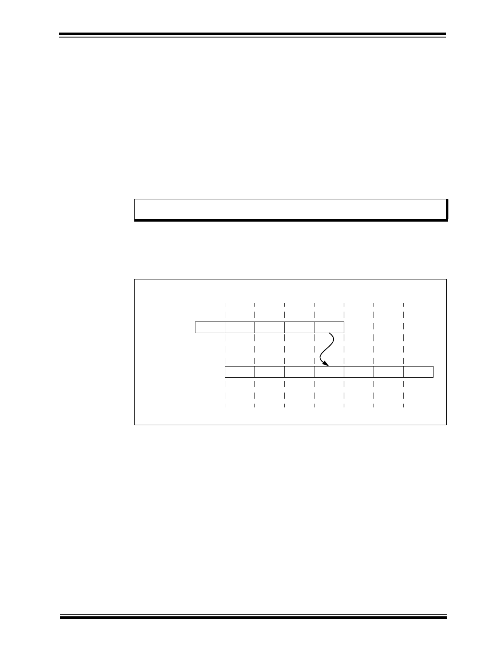
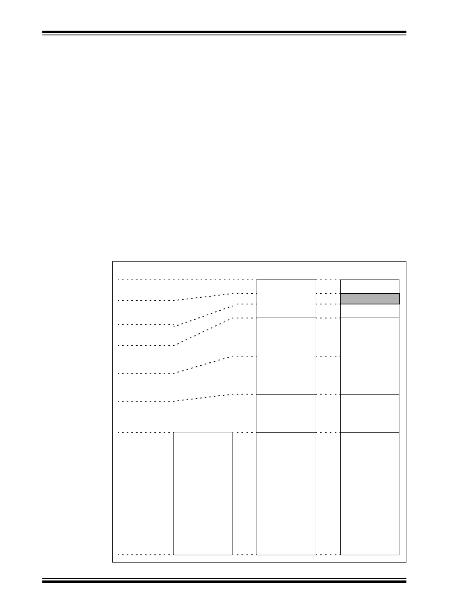
As shown in Figure 50-6, the sub instruction has a source operand dependency on register r3
with the previous add instruction. The sub instruction slips by two clocks waiting until the result
of the add is written back to register r3. This slipping does not occur on the PIC32 family of
processors.
Figure 50-6: Pipeline Slip (If Bypassing Was Not Implemented)
Note: To illustrate the concept of a pipeline slip, the example in Figure 50-6 shows would
happen if the PIC32 core did not implement register bypassing.
EI M W
E
SLIP
I M A WE
One
Cycle
One
Cycle
One
Cycle
One
Cycle
One
Cycle
One
Cycle
One
Cycle
One
Cycle
A
E
SLIP
Add r3, r2, r1
(r r3 2 + r1
Sub r4, r3, r7
(r r4 3 – r7
PIC32 Family Reference Manual
DS60001192B-page 50-12 © 2013-2015 Microchip Technology Inc.
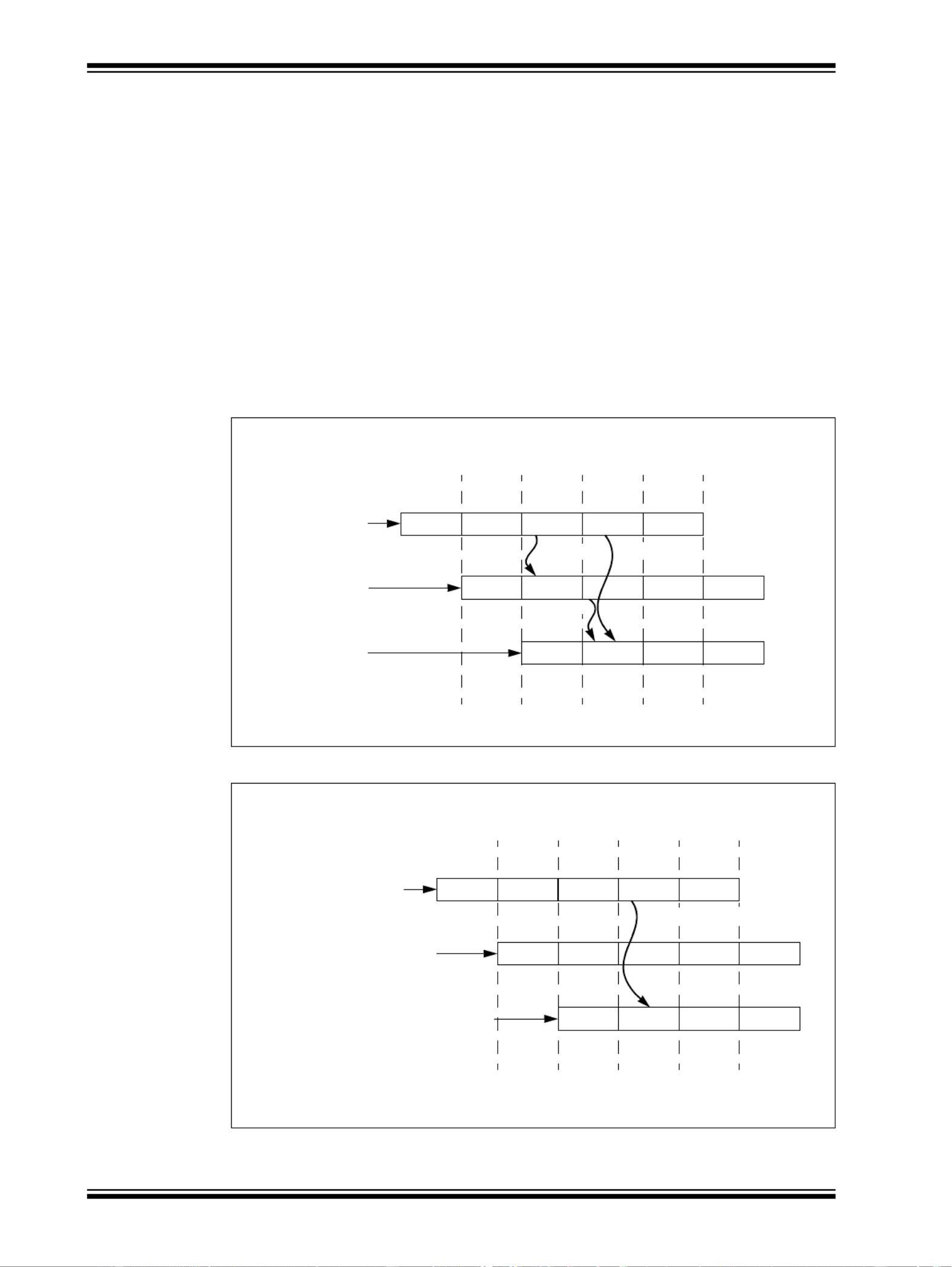
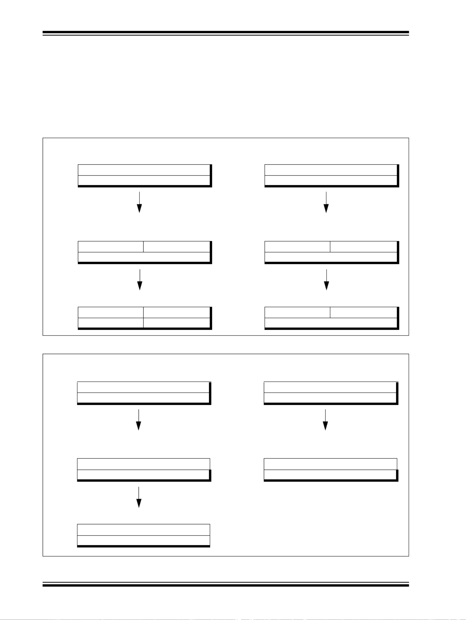
50.3.6 Register Bypassing
As mentioned previously, the PIC32 processor implements a mechanism called register bypass-
ing that helps reduce pipeline slips during execution. When an instruction is in the E stage of the
pipeline, the operands must be available for that instruction to continue. If an instruction has a
source operand that is computed from another instruction in the execution pipeline, register
bypassing allows a shortcut to get the source operands directly from the pipeline. An instruction
in the E stage can retrieve a source operand from another instruction that is executing in either
the M stage or the A stage of the pipeline. As seen in Figure 50-7, a sequence of three instruc-
tions with interdependencies does not slip at all during execution. This example uses both A to
E, and M to E register bypassing. Figure 50-8 shows the operation of a load instruction utilizing
A to E bypassing. Since the result of load instructions are not available until the A pipeline stage,
M to E bypassing is not needed.
The performance benefit of register bypassing is that instruction throughput is increased to the
rate of one instruction per clock for ALU operations, even in the presence of register
dependencies.
Figure 50-7: IU Pipeline M to E Bypass
Figure 50-8: IU Pipeline A to E Data Bypass
EI M W
EI WA
One
Cycle
One
Cycle
One
Cycle
One
Cycle
One
Cycle
One
Cycle
A
M
Add
1
r r r3 = 2 + 1
Sub
2
r r r4 = 3 – 7
Add
3
r r r5 = 3 + 4 EI AM
M to E Bypass A to E Bypass
M to E Bypass
EI M W
EI WA
One
Cycle
One
Cycle
One
Cycle
One
Cycle
One
Cycle
One
Cycle
A
M
Load Instruction
Consumer of Load Data Instruction
EI AM
Data Bypass from A to E
One Clock
Load Delay

PIC32 Family Reference Manual
DS60001192B-page 50-14 © 2013-2015 Microchip Technology Inc.
50.5 MIPS32 ARCHITECTURE
The MIPS32 architecture is based on a fixed-length, regularly encoded instruction set and uses
a load/store data model. The architecture is streamlined to support optimized execution of
high-level languages. Arithmetic and logic operations use a three-operand format, allowing
compilers to optimize complex expressions formulation. Availability of 32 general-purpose
registers enables compilers to further optimize code generation for performance by keeping
frequently accessed data in registers.
For more information and documentation, refer to the MIPS32 Architecture web page at:
http://www.imgtec.com/mips/architectures/mips32.asp
50.5.1 Architecture Release 2
PIC32 devices with the microAptiv core utilize Release 2 of the MIPS32 processor architecture,
and implement the following features:
• Vectored interrupts using and external-to-core interrupt controller, which provides the ability
to vector interrupts directly to a handler for that interrupt
• Programmable exception vector base, which allows the base address of the exception
vectors to be moved for exceptions that occur when Status
BEV
is ‘0’. This feature enables
any system to place the exception vectors in memory that is appropriate to the system
environment.
• Atomic interrupt enable/disable, which includes two added instructions to atomically enable
or disable interrupts, and return the previous value of the Status register
• The ability to disable the Count register for highly power-sensitive applications
• GPR shadow registers, which provide the addition of GPR shadow registers and the ability
to bind these registers to a vectored interrupt or exception
• Field, Rotate, and Shuffle instructions, which add additional capability in processing bit
fields in registers
• Explicit hazard management, which provides a set of instructions to explicitly manage
hazards, in place of the cycle-based SSNOP method of dealing with hazards
50.5.2 Architecture Release 5
PIC32 devices with the M-Class core utilize all of the features of Release 2, as well as the
following Release 5 features:
• User mode access through the UFR bit in the Config5 Register (CP0 Register 16, Select 5)
• Additional MCU ASE instructions: ASET and ACLR for setting and clearing atomic 8-bit
memory locations

© 2013-2015 Microchip Technology Inc. DS60001192B-page 50-15
Section 50. CPU for Devices with MIPS32
®
microAptiv™ and M-Class Cores
50.6 CPU BUS
The PIC32 devices use two different CPU bus architectures, either split-bus or data/instruction
bus, depending on which CPU core is implemented.
50.6.1 Split-bus Architecture
PIC32 devices based on the MCU Microprocessor core have a Split-bus architecture, with two
distinct busses to provide parallel instruction and data operations. Load and store operations
occur simultaneously as instruction fetches. The two busses are known as the I-side bus, which
is used for feeding instructions into the CPU, and the D-side bus, which is used for data transfers.
In the split-bus architecture, the CPU fetches instructions during the I-pipeline stage. A fetch is
issued to the I-side bus and is handled by the System Bus. Depending on the address, the
System Bus will do one of the following:
• Forward the fetch request to the Prefetch Cache unit (if available)
• Forward the fetch request to the DRM unit, or
• Cause an exception
Instruction fetches always use the I-side bus independent of the addresses being fetched.
The D-side bus processes all load and store operations executed by the CPU. When a load or
store instruction is executed, the request is routed to the System Bus by the D-side bus. This
operation occurs during the M-pipeline stage and is routed to one of several targets:
• Data RAM
• Prefetch Cache/Flash memory
• Fast Peripheral Bus (Interrupt controller, DMA, Debug unit, USB, Ethernet, GPIO ports)
• General Peripheral Bus (UART, SPI, Flash Controller, EPMP/EPSP, TRCC Timers, Input
Capture, PWM/Output Compare, ADC, Dual Compare, I
2
C, Clock SIB, and Reset SIB)
50.6.2 Data/Instruction Architecture
PIC32 devices based on the MPU core have a unified Data or Instruction bus connected to the
System Bus. This architecture uses a multi-layer System Bus to provide multiple simultaneous
data transactions between bus initiators and targets.
50.7 INTERNAL SYSTEM BUSSES
The internal busses of the PIC32 processor connect the peripherals to the System Bus. The
System Bus routes bus accesses from different initiators to a set of targets utilizing several data
paths throughout the device to help eliminate performance bottlenecks.
Some of the paths that the System Bus uses serve a dedicated purpose, while others are shared
between several targets.
The data RAM and Flash memory read paths are dedicated paths, allowing low-latency access
to the memory resources without being delayed by peripheral bus activity. The high-bandwidth
peripherals are placed on a high-speed bus. These include the Interrupt controller, Debug unit,
DMA engine, the USB Host/Peripheral unit, and other high-bandwidth peripherals (i.e., CAN,
Ethernet engines).
Peripherals that do not require high-bandwidth are located on a separate peripheral bus to save
power.
PIC32 Family Reference Manual
DS60001192B-page 50-16 © 2013-2015 Microchip Technology Inc.
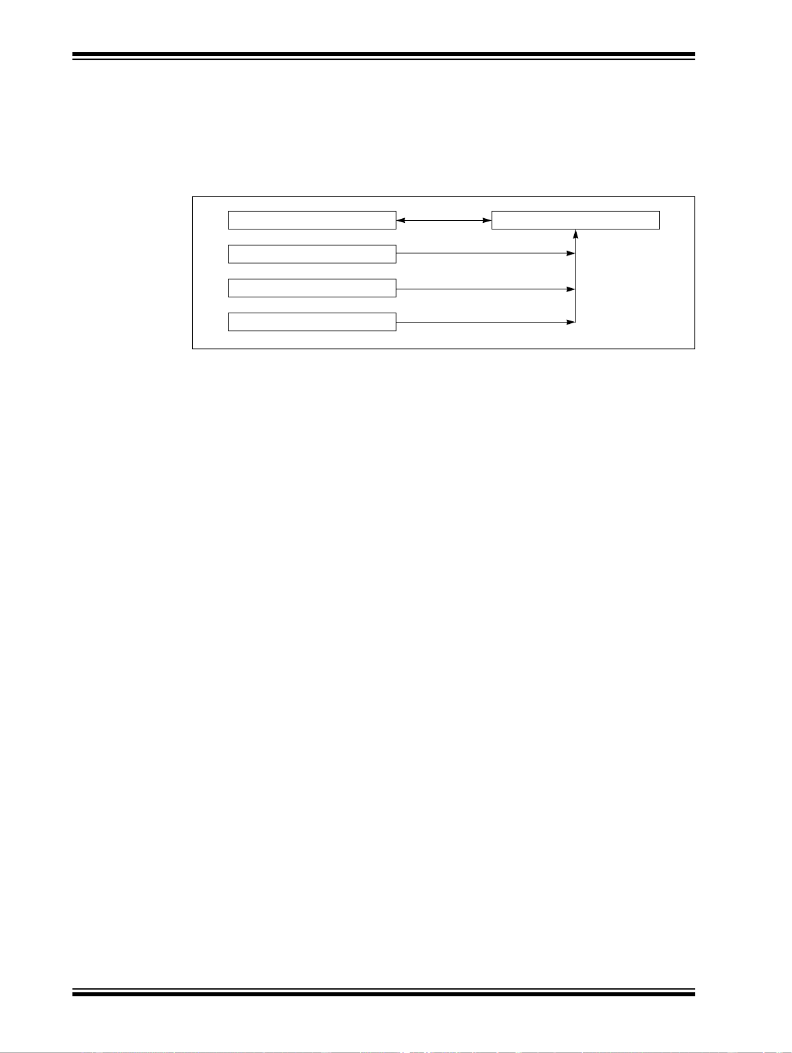
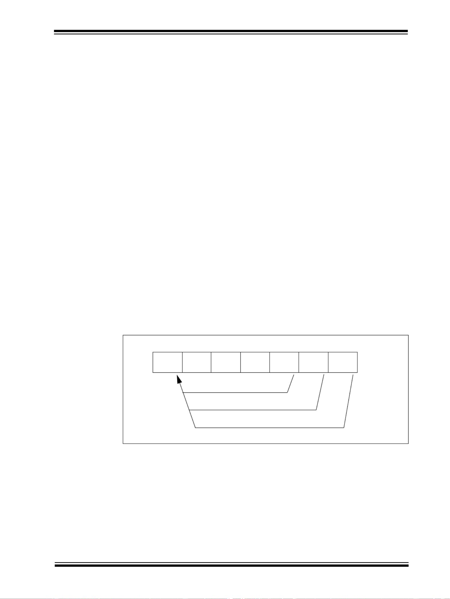
50.8 SET/CLEAR/INVERT
To provide single-cycle bit operations on peripherals, the registers in the peripheral units can be
accessed in three different ways depending on peripheral addresses. Each register has four dif-
ferent addresses. Although the four different addresses appear as different registers, they are
really just four different methods to address the same physical register.
Figure 50-9: Four Addresses for a Single Physical Register
The base register address provides normal Read/Write access, while the other three provide
special write-only functions.
• Normal access
• Set bit atomic RMW access
• Clear bit atomic RMW access
• Invert bit atomic RMW access
Peripheral reads must occur from the base address of each peripheral register. Reading from a
Set/Clear/Invert address has an undefined meaning, and may be different for each peripheral.
Writing to the base address writes an entire value to the peripheral register. All bits are written.
For example, assume a register contains 0xAAAA5555 before a write of 0x000000FF. After the
write, the register will contain 0x000000FF (assuming that all bits are R/W bits).
Writing to the Set address for any peripheral register causes only the bits written as ‘1’s to be set
in the destination register. For example, assume that a register contains 0xAAAA5555 before a
write of 0x000000FF to the set register address. After the write to the Set register address, the
value of the peripheral register will contain 0xAAAA55FF.
Writing to the Clear address for any peripheral register causes only the bits written as ‘1’s to be
cleared to ‘0’s in the destination register. For example, assume that a register contains
0xAAAA5555 before a write of 0x000000FF to the Clear register address. After the write to the
Clear register address, the value of the peripheral register will contain 0xAAAA5500.
Writing to the Invert address for any peripheral register causes only the bits written as ‘1’s to be
inverted, or toggled, in the destination register. For example, assume that a register contains
0xAAAA5555 before a write of 0x000000FF to the invert register address. After the write to the
Invert register, the value of the peripheral register will contain 0xAAAA55AA.
50.9 ALU STATUS BITS
Unlike most other PIC microcontrollers, the PIC32 processor does not use Status register flags.
Condition flags are used on many processors to help perform decision making operations during
program execution. Flags are set based on the results of comparison operations or some arith-
metic operations. Conditional branch instructions on these machines then make decisions based
on the values of the single set of condition codes.
Instead, the PIC32 processor uses instructions that perform a comparison and stores a flag or
value into a General Purpose Register. A conditional branch is then executed with this general
purpose register used as an operand.
Peripheral RegisterRegister Address
Register Address + 4
Register Address + 8
Register Address + 12
Clear Bits
Set Bits
Invert Bits

© 2013-2015 Microchip Technology Inc. DS60001192B-page 50-17
Section 50. CPU for Devices with MIPS32
®
microAptiv™ and M-Class Cores
50.10 INTERRUPT AND EXCEPTION MECHANISM
The PIC32 family of processors implement an efficient and flexible interrupt and exception han-
dling mechanism. Interrupts and exceptions both behave similarly in that the current instruction
flow is changed temporarily to execute special procedures to handle an interrupt or exception.
The difference between the two is that interrupts are usually a result of normal operation, and
exceptions are a result of error conditions such as bus errors.
When an interrupt or exception occurs, the processor does the following:
1. The PC of the next instruction to execute after the handler returns is saved into a
coprocessor register.
2. The Cause register is updated to reflect the reason for exception or interrupt.
3. The Status register EXL or ERL bit is set to cause Kernel mode execution.
4. Handler PC is calculated from Ebase and OFFSET values.
5. Automated Interrupt Epilogue can save some of the COP0 state in the stack and
automatically update some of the COP0 registers in preparation for interrupt handling.
6. Processor starts execution from new PC.
This is a simplified overview of the interrupt and exception mechanism. Refer to the “CPU
Exceptions and Interrupt Controller” chapter in the specific device data sheet for details.
50.11 PROGRAMMING MODEL
The PIC32 family of processors is designed to be used with a high-level language such as the C
programming language. It supports several data types and uses simple but flexible addressing
modes needed for a high-level language. There are 32 General Purpose Registers and two
special registers for multiplying and dividing.
There are three different formats for the machine language instructions on the PIC32 processor:
• Immediate or I-type CPU instructions
• Jump or J-type CPU instructions, and
• Registered or R-type CPU instructions
Most operations are performed in registers. The register type CPU instructions have three
operands; two source operands and a destination operand.
Having three operands and a large register set allows assembly language programmers and
compilers to use the CPU resources efficiently. This creates faster and smaller programs by
allowing intermediate results to stay in registers rather than constantly moving data to and from
memory.
The immediate format instructions have an immediate operand, a source operand and a desti-
nation operand. The jump instructions have a 26-bit relative instruction offset field that is used to
calculate the jump destination.
Note: In this section, the terms “precise” and “imprecise” are used to describe exceptions.
A precise exception is one in which the EPC (CP0, Register 14, Select 0) can be
used to identify the instruction that caused the exception. For imprecise exceptions,
the instruction that caused the exception cannot be identified. Most exceptions are
precise. Bus error exceptions may be imprecise.

PIC32 Family Reference Manual
DS60001192B-page 50-18 © 2013-2015 Microchip Technology Inc.
50.11.1 CPU Instruction Formats
A CPU instruction is a single 32-bit aligned word. The CPU instruction formats are:
• Immediate (see Figure 50-10)
• Jump (see Figure 50-11)
• Register (see Figure 50-12)
Table 50-4 describes the fields used in these instructions.
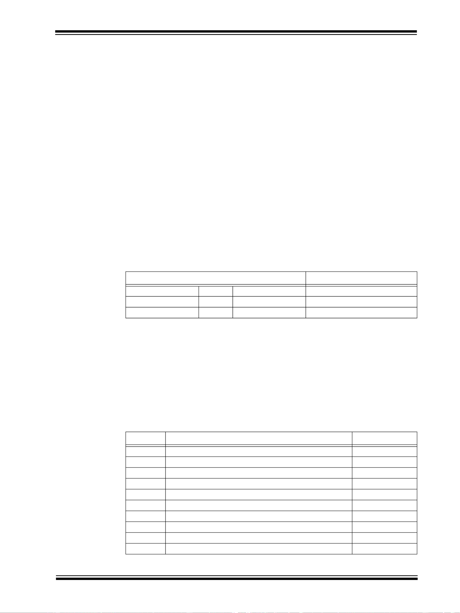
Table 50-4: CPU Instruction Format Fields
Figure 50-10: Immediate (I-Type) CPU Instruction Format
Figure 50-11: Jump (J-Type) CPU Instruction Format
Figure 50-12: Register (R-Type) CPU Instruction Format
Field Description
opcode 6-bit primary operation code.
rd 5-bit specifier for the destination register.
rs 5-bit specifier for the source register.
rt 5-bit specifier for the target (source/destination) register or used to specify
functions within the primary opcode REGIMM.
immediate 16-bit signed immediate used for logical operands, arithmetic signed operands,
load/store address byte offsets, and PC-relative branch signed instruction
displacement.
instr_index 26-bit index shifted left two bits to supply the low-order 28 bits of the jump
target address.
sa 5-bit shift amount.
function 6-bit function field used to specify functions within the primary opcode
SPECIAL.
31 26 25 21 20 16 15 0
opcode rs rt immediate
6 5 5 16
31 26 25 21 20 16 15 11 10 6 5 0
opcode instr_index
6 26
31 26 25 21 20 16 15 11 10 6 5 0
opcode rs rt rd sa function
6 5 5 5 5 6

© 2013-2015 Microchip Technology Inc. DS60001192B-page 50-19
Section 50. CPU for Devices with MIPS32
®
microAptiv™ and M-Class Cores
50.11.2 CPU Registers
The PIC32 architecture defines the following CPU registers:
• Thirty-two 32-bit General Purpose Registers (GPRs)
• The standard MIPS32 architecture defines one pair of HI/LO accumulator registers (AC0).
The cores in PIC32 devices include the DSP ASE (see Note), which provides three addi-
tional pairs of HI/LO accumulator registers (AC1, AC2, and AC3). These registers improve
the parallelization of independent accumulation routines. DSP instructions that target the
accumulators use two instruction bits to specify the destination accumulator.
• A special purpose program counter (PC), which is affected only indirectly by certain
instructions; it is not an architecturally visible register.
50.11.2.1 CPU GENERAL PURPOSE REGISTERS
Two of the CPU General Purpose Registers have assigned functions:
• r0 – This register is hard-wired to a value of ‘0’, and can be used as the target register for
any instruction the result of which will be discarded. r0 can also be used as a source when
a ‘0’ value is needed.
• r31 – This is the destination register used by JAL, BLTZAL, BLTZALL, BGEZAL, and
BGEZALL, without being explicitly specified in the instruction word; otherwise, r31 is used
as a normal register.
The remaining registers are available for general purpose use.
50.11.2.2 REGISTER CONVENTIONS
Although most of the registers in the PIC32 architecture are designated as General Purpose
Registers, as shown in Table 50-5, there are some recommended uses of the registers for correct
software operation with high-level languages such as the Microchip MPLAB
®
XC32 C/C++
compiler.
Table 50-5: Register Conventions
Note: DSP ASE is not available on all devices. Please consult the “CPU” chapter of the
specific device data sheet to determine availability
CPU
Register
Symbolic
Register Usage
r0 zero Always ‘0’ (see Note 1)
r1 at Assembler Temporary
r2 - r3 v0-v1 Function Return Values
r4 - r7 a0-a3 Function Arguments
r8 - r15 t0-t7 Temporary – Caller does not need to preserve contents
r16 - r23 s0-s7 Saved Temporary – Caller must preserve contents
r24 - r25 t8-t9 Temporary – Caller does not need to preserve contents
r26 - r27 k0-k1 Kernel temporary – Used for interrupt and exception handling
r28 gp Global Pointer – Used for fast-access common data
r29 sp Stack Pointer – Software stack
r30 s8 or fp Saved Temporary – Caller must preserve contents OR
Frame Pointer – Pointer to procedure frame on stack
r31 ra Return Address (see Note 1)
Note 1: Hardware enforced, not just convention.

PIC32 Family Reference Manual
DS60001192B-page 50-20 © 2013-2015 Microchip Technology Inc.
50.11.2.3 CPU SPECIAL PURPOSE REGISTERS
The CPU contains these special purpose registers:
• PC – Program Counter register
• AC0 through AC3 – 64-bit Accumulator register pairs (HI/LO):
- HI/LO – Multiply and divide register pair (high and low result):
• During a multiply operation, the HI and LO registers store the product of integer multiply
• During a multiply-add or multiply-subtract operation, the HI and LO registers store the
result of the integer multiply-add or multiply-subtract
• During a division, the HI and LO registers store the quotient (in LO) and remainder (in
HI) of integer divide
• During a multiply-accumulate, the HI and LO registers store the accumulated result of
the operation
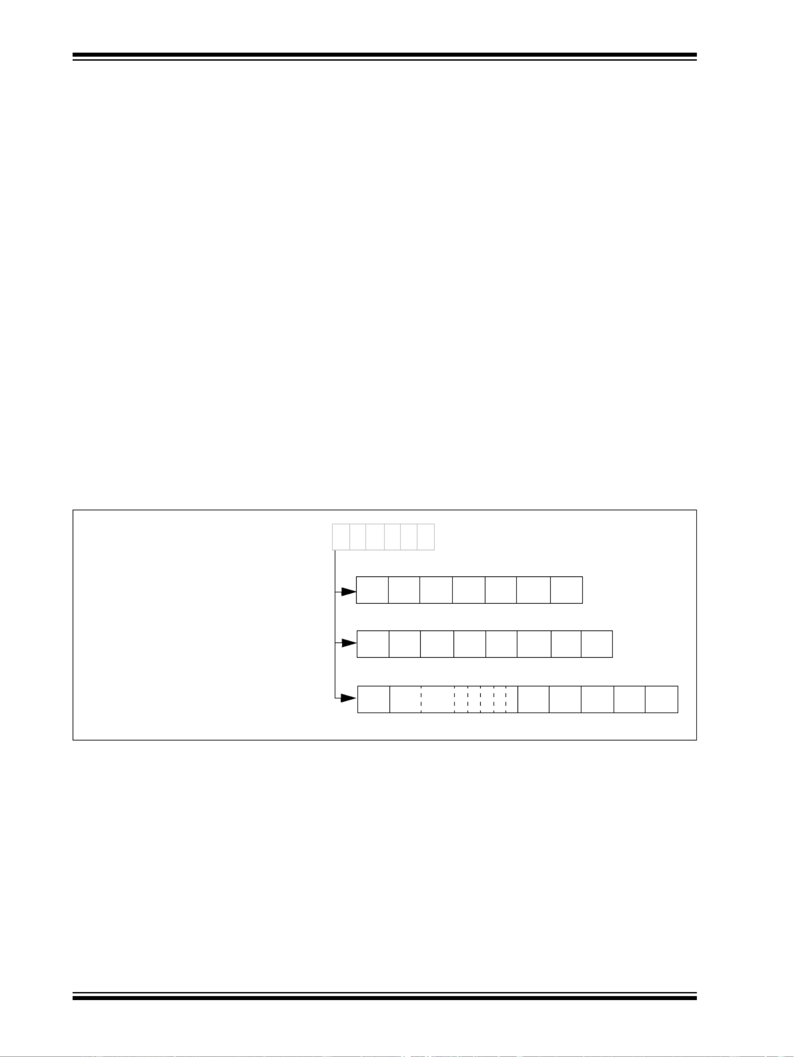
Figure 50-13 shows the layout of the CPU registers.
Figure 50-13: CPU Registers
31 0 31 0
r0 (zero) HI (0)
r1 (at) LO (0)
r2 (v0) HI (1)
r3 (v1) LO (1)
r4 (a0) HI (2)
r5 (a1) LO (2)
r6 (a2) HI (3)
r7 (a3) LO (3)
r8 (t0)
r9 (t1)
r10 (t2)
r11 (t3)
r12 (t4)
r13 (t5)
r14 (t6)
r15 (t7)
r16 (s0)
r17 (s1)
r18 (s2)
r19 (s3)
r20 (s4)
r21 (s5)
r22 (s6)
r23 (s7)
r24 (t8)
r25 (t9)
r26 (k0)
r27 (k1)
r28 (gp)
r29 (sp)
r30 (s8 or fp) 31 0
r31 (ra) PC
General Purpose Registers Special Purpose Registers

© 2013-2015 Microchip Technology Inc. DS60001192B-page 50-21
Section 50. CPU for Devices with MIPS32
®
microAptiv™ and M-Class Cores
Table 50-6: microMIPS 16-bit Instruction Register Usage
Table 50-7: microMIPS Special Registers
16-bit
Register
Encoding
32-bit MIPS
Register
Encoding
Symbolic
Name Description
0 16/0 s0/zero General-purpose register
1 17 s1 General-purpose register
2 2 v0 General-purpose register
3 3 v1 General-purpose register
4 4 a0 General-purpose register
5 5 a1 General-purpose register
6 6 a2 General-purpose register
7 7 a3 General-purpose register
N/A 28 gp microMIPS implicitly referenced
General-pointer register
N/A 29 sp microMIPS implicitly referenced Stack
pointer register
N/A 31 ra microMIPS implicitly referenced Return
address register
Symbolic
Name Purpose
PC Program counter. The PC-relative instructions can access this register as an
operand.
HI Contains high-order word of multiply or divide result.
LO Contains low-order word of multiply or divide result.
PIC32 Family Reference Manual
DS60001192B-page 50-22 © 2013-2015 Microchip Technology Inc.
50.11.3 How to Implement Stack/MIPS Calling Conventions
The PIC32 CPU does not have hardware stacks. Instead, the processor relies on software to pro-
vide this functionality. Since the hardware does not perform stack operations itself, a convention
must exist for all software within a system to use the same mechanism. For example, a stack can
grow either toward lower addresses, or grow toward higher addresses. If one piece of software
assumes that the stack grows toward a lower address, and calls a routine that assumes that the
stack grows toward a higher address, the stack would become corrupted.
Using a system-wide calling convention prevents this problem from occurring. The Microchip
MPLAB
®
XC32 C/C++ Compiler assumes the stack grows toward lower addresses.
50.11.4 Processor Modes
There are two operational modes and one special mode of execution in the PIC32 family CPUs:
User mode, Kernel mode and Debug mode. The processor starts execution in Kernel mode, and
if desired, can stay in Kernel mode for normal operation. User mode is an optional mode that
allows a system designer to partition code between privileged and unprivileged software. Debug
mode is normally only used by a debugger or monitor.
One of the main differences between the modes of operation is the memory addresses that soft-
ware is allowed to access. Peripherals are not accessible in User mode. Figure 50-14 shows the
different memory maps for each mode. For more information on the processor’s memory map,
refer to Section 3. “Memory Organization” (DS60001115) of the “PIC32 Family Reference
Manual”.
Figure 50-14: CPU Modes
useg kuseg kuseg
kseg0
kseg1
kseg2
kseg3
kseg2
kseg1
kseg0
kseg3
kseg3
dseg
User Mode Kernel Mode Debug ModeVirtual Address
0x7FFF_FFFF
0x8000_0000
0x9FFF_FFFF
0xBFFF_FFFF
0xDFFF_FFFF
0xFF1F_FFFF
0xFF3F_FFFF
0xFFFF_FFFF
0xA000_0000
0xC000_0000
0xE000_0000
0xFF20_0000
0xFF40_0000
0x0000_0000

© 2013-2015 Microchip Technology Inc. DS60001192B-page 50-23
Section 50. CPU for Devices with MIPS32
®
microAptiv™ and M-Class Cores
50.11.4.1 KERNEL MODE
To access many of the hardware resources, the processor must be operating in Kernel mode.
Kernel mode gives software access to the entire address space of the processor as well as
access to privileged instructions.
The processor operates in Kernel mode when the DM bit in the Debug register is ‘0’ and the Status
register contains one, or more, of the following values:
• UM = 0
• ERL = 1
• EXL = 1
When a non-debug exception is detected, EXL or ERL will be set and the processor will enter
Kernel mode. At the end of the exception handler routine, an Exception Return (ERET) instruction
is generally executed. The ERET instruction jumps to the Exception PC (EPC or ErrorPC
depending on the exception), clears ERL, and clears EXL if ERL= 0.
If UM = 1 the processor will return to User mode after returning from the exception when ERL
and EXL are cleared back to ‘0’.
50.11.4.2 USER MODE
When executing in User mode, software is restricted to use a subset of the processor’s
resources. In many cases it is desirable to keep application-level code running in User mode
where if an error occurs it can be contained and not be allowed to affect the Kernel mode code.
Applications can access Kernel mode functions through controlled interfaces such as the
SYSCALL mechanism.
As seen in Figure 50-14, User mode software has access to the USEG memory area.
To operate in User mode, the Status register must contain each the following bit values:
• UM = 1
• EXL = 0
• ERL = 0
50.11.4.3 DEBUG MODE
Debug mode is a special mode of the processor normally only used by debuggers and system
monitors. Debug mode is entered through a debug exception and has access to all Kernel mode
resources as well as special hardware resources used to debug applications.
The processor is in Debug mode when the DM bit in the Debug register is ‘1’.
Debug mode is normally exited by executing a DERET instruction from the debug handler.

PIC32 Family Reference Manual
DS60001192B-page 50-24 © 2013-2015 Microchip Technology Inc.
50.12 FLOATING POINT UNIT (FPU)
PIC32 devices with the M-Class core contain a Floating Point Unit (FPU) that implements the
MIPS Release 5 Instruction Set Architecture for floating point computation.
50.12.1 Features
Some of the most important features of this module include:
• The PIC32 implementation supports the “IEEE Standard for Binary Floating-Point
Arithmetic” (ANSI/IEEE 754 Standard) for single and double precision data formats. See
50.12.6.5 “IEEE 754-1985 Standard” for more information.
• Full 64-bit operation is implemented in both the register file and functional units. The FPU
has 32 64-bit floating point registers used for all of the floating point operations.
• A 32-bit Floating Point Control Register controls the operation of the FPU, and monitors
condition codes and exception conditions
• The performance of the unit is optimized for single precision formats. Most instructions have
one FPU cycle throughput and four FPU cycle latency.
• The FPU implements compound multiply-add (MADD) and multiply-sub (MSUB) instructions
with intermediate rounding after the multiply function. The result is guaranteed to be the
same as executing a MUL followed by an ADD SUB/ instruction, but the instruction latency,
instruction fetch, dispatch bandwidth, and the total number of register accesses is improved.
• IEEE denormalized input operands and results are supported by hardware for some
instructions. A fast flush-to-zero mode is provided to optimize performance for IEEE
denormalized results. The fast flush-to-zero mode has to be enabled through the FPU
control registers, and use of this mode is recommended for best performance when
denormalized results are generated.
• Additional arithmetic operations not specified by IEEE 754 Standard (for example, reciprocal
and reciprocal square root) are specified by the MIPS
®
architecture (see Note) and are
implemented by the FPU. To achieve low latency counts, these instructions satisfy more
relaxed precision requirements.
• The MIPS FPU architecture is designed such that a combination of hardware and software
can be used to implement the architecture. The PIC32 FPU can operate on numbers within
a specific range (the IEEE normalized numbers), but it relies on a software handler to
operate on numbers not handled by the FPU hardware (the IEEE denormalized numbers).
• The FPU has a separate pipeline for floating point instruction execution. This pipeline
operates in parallel with the integer core pipeline and does not stall when the integer
pipeline stalls. This allows long-running FPU operations, such as divide or square root, to
be partially masked by system stalls and/or other integer unit instructions.
• The FPU access is provided through Coprocessor 1. Like the main processor core,
Coprocessor 1 is programmed and operated using a Load/Store instruction set. The
processor core communicates with Coprocessor 1 using a dedicated coprocessor interface.
The FPU functions as an autonomous unit. The hardware is completely interlocked such
that, when writing software, the programmer does not have to worry about inserting delay
slots after loads and between dependent instructions.
• Arithmetic instructions are always dispatched and completed in order, but loads and stores
can complete out of order. The exception model is ‘precise’ at all times.
Refer to 50.14 “Coprocessor 1 (CP1) Registers” for information on the related FPU registers.
Figure 50-15 shows a block diagram of the PIC32 FPU.
Note: This module is not available on all devices. Refer to the “CPU” chapter in the
specific device data sheet to determine availability.
Note: Refer to the Imagination Technologies Ltd. website, www.imgtec.com, for
information on the MIPS architecture.

PIC32 Family Reference Manual
DS60001192B-page 50-26 © 2013-2015 Microchip Technology Inc.
Table 50-8: Parameters of Floating Point Data Types
Figure 50-16: Single-Precision Floating Point Format (S)
Figure 50-17: Double-Precision Floating Point Format (D)
The fields in the Figure 50-16 and Figure 50-16 are:
• 1-bit sign, S
• Biased exponent, e = E + bias
• Binary fraction, f =.b1 b2..bp-1 (the b0 bit is hidden; it is not recorded)
Values are encoded in the specified format using the unbiased exponent, fraction, and sign
values listed in Table 50-9.
The high-order bit of the Fraction field, identified as b1, has also special importance for NaNs.
Parameter Single Double
Bits of mantissa precision, p 24 53
Maximum exponent, E_max +127 +1023
Minimum exponent, E_min -126 -1022
Exponent bias +127 +1023
Bits in exponent field, e 8 11
Representation of b0 integer
bit
Hidden Hidden
Bits in fraction field, f 23 52
Total format width in bits 32 64
Magnitude of largest repre-
sentable number
3.4028234664e+38 1.7976931349e+308
Magnitude of smallest normal-
ized representable number
1.1754943508e-38 2.2250738585e-308
S Exponent <0:7> Fraction <0:22>
S Exponent <0:10> Fraction <0:51>

PIC32 Family Reference Manual
DS60001192B-page 50-28 © 2013-2015 Microchip Technology Inc.
50.12.2.2 INFINITY ARITHMETIC
Infinity represents a number with magnitude too large to be represented in the given format.
During a computation it represents a magnitude overflow. A correctly signed +
∞
or -
∞
will be
generated as the default result in division by zero operations and some cases of overflow as
described in 50.12.5 “Floating Point Exceptions Overview”.
When created as a default result, ∞ can become an operand in a subsequent operation. The
ordering is such that -
∞
< (every finite number) < +
∞
. Arithmetic with
∞
is the limiting case of
real arithmetic with operands of arbitrarily large magnitude, when such limits exist. In these
cases, arithmetic on
∞
is regarded as exact, and exception conditions do not arise. The
out-of-range indication represented by
∞
is propagated through subsequent computations.
For some cases, there is no meaningful limiting case in real arithmetic for operands of
∞
. These
cases raise the Invalid Operation exception condition as described in 50.12.3 “General Floating
Point Registers”.
50.12.2.2.1 Signaling Non-Number (SNaN)
SNaN operands cause an Invalid Operation exception for arithmetic operations. SNaNs are
useful values to put in uninitialized variables. A SNaN is never produced as a result value.
The MIPS architecture makes the formatted operand move instructions (MOV.fmt MOVT.fmt, ,
MOVF.fmt MOVN.fmt MOVZ.fmt, , ) non-arithmetic; they do not signal IEEE 754 Standard
exceptions.
50.12.2.2.2Quiet Non-Number (QNaN)
QNaNs provide diagnostic information propagated from invalid or unavailable data and results.
This propagation requires that the information contained in a QNaN be preserved through
arithmetic operations and floating point format conversions.
Arithmetic operations with QNaN operands do not signal an exception. When a floating point
result is to be delivered, a QNaN operand causes an arithmetic operation to supply a QNaN
result. When possible, this QNaN result is one of the operand QNaN values.
QNaNs have similar effects to SNaNs on operations that do not deliver a floating point result (i.e.,
comparison operations).
When certain invalid operations not involving QNaN operands are performed and the trap is not
enabled, a new QNaN value is created. Table 50-10 shows the QNaN value generated when no
input operand QNaN value can be copied. The values listed for the fixed point formats are the
values supplied to satisfy the IEEE 754 Standard when a QNaN or infinite floating point value is
converted to fixed point. There is no other feature of the architecture that detects or utilizes these
“integer QNaN” values.
Table 50-10: Value Supplied When a New QNaN is Created
50.12.2.3 FIXED POINT FORMATS
The PIC32 FPU provides two fixed point data types which are the signed integers that are
provided by the MIPS architecture:
• 32-bit Word Fixed Point Format (type W)
• 64-bit Long Word Fixed Point Format (type L)
The fixed point values are held in 2’s complement format, which is used for signed integers in the
CPU. Unsigned fixed point data types are not provided by the architecture; application software
can synthesize computations for unsigned integers from the existing instructions and data types.
Format New QNan Value
(FCSR
NAN
2008 = 0)
New QNaN Value
(FCSR
NAN
2008 = 1)
Single floating point 0x7FBF FFFF 0x7FFF FFFF
Double floating point 0x7FF7 FFFF FFFF FFFF 0x7FFF FFFF FFFF FFFF
Word fixed point 0x7FFF FFFF 0x7FFF FFFF
Long word fixed point 0x7FFF FFFF FFFF FFFF 0x7FFF FFFF FFFF FFFF
PIC32 Family Reference Manual
DS60001192B-page 50-30 © 2013-2015 Microchip Technology Inc.
50.12.3.3 32-BIT AND 64-BIT BINARY DATA TRANSFER
The data transfer instructions move words and double words between the FPU FPRs and the
system.
The operations of the word and double word load and move-to instructions are shown in
Figure 50-20 and Figure 50-21, respectively.
The store and move-from instructions do the reverse, reading data from the location that the
corresponding load or move-to instruction had written.
Figure 50-20: FPU Word Load and Move-to Operations
Figure 50-21: FPU Double Word Load and Move-to Operations
FR bit = FR bit = 1 0
63 0 63 0
Reg 0 Initial Value 1 Reg 0 Initial Value 1
Reg 1 Initial Value 2 Reg 2 Initial Value 2
LWC1 f0, 0(r0) / MTC1 f0, r0
63 0 63 0
Reg 0 Undefined/Unused Data Word (0) Reg 0 Undefined/Unused Data Word (0)
Reg 1 Initial Value 2 Reg 2 Initial Value 2
LWC1 f1, 4(r0) / MTC1 f1, r4
63 0 63 0
Reg 0 Undefined/Unused Data Word (0) Reg 0 Data Word (4) Data Word (0)
Reg 1 Undefined/Unused Data Word (4) Reg 2 Initial Value 2
FR bit = 1FR bit = 0
63 0 63 0
Reg 0 Initial Value 1 Reg 0 Initial Value 1
Reg 1 Initial Value 2 Reg 2 Initial Value 2
LDC1 f0, 0(r0)
63 0 63 0
Reg 0 Data Double Word (0) Reg 0 Data Double Word (0)
Reg 1 Initial Value 2 Reg 2 Initial Value 2
LDC1 f1, 8(r0)
63 0
Reg 0 Data Double Word (0) (Illegal when FR bit = 0)
Reg 1 Data Double Word (9)
© 2013-2015 Microchip Technology Inc. DS60001192B-page 50-31
Section 50. CPU for Devices with MIPS32
®
microAptiv™ and M-Class Cores
50.12.4 Floating Point Instruction Overview
The FPU instructions are divided into these categories:
•FPU Data Transfer Instructions
•FPU Arithmetic Instructions
•FPU Conversion Instructions
•FPU Formatted Operand-Value Move Instructions
•FPU Conditional Branch Instructions
•FPU Miscellaneous Instructions
The instructions are described in detail in Chapter 14, “M5150 Processor Core Instructions”
of the “MIPS32
®
M5150 Processor Core Family Software User’s Manual”. This document is
available for download by registered users from the Imagination Technologies Ltd. website
(www.imgtec.com).
50.12.4.1 FPU DATA TRANSFER INSTRUCTIONS
The FPU has two register sets: Coprocessor General Registers (FPRs) and Coprocessor Control
Registers (FCRs). The FPU has a load/store architecture: all computations are done on data held
in coprocessor general registers.
The control registers are used to control FPU operation. Data is transferred between registers
and the rest of the system with dedicated load, store, and move instructions. The transferred data
is treated as unformatted binary data. No format conversions are performed, and therefore no
IEEE floating point exceptions can occur.
Table 50-11: FPU Data Transfer Instructions
All coprocessor loads and stores operate on naturally aligned data items. An attempt to load or
store to an address that is not naturally aligned for the data item causes an Address Error
exception. The address of a word or double word is the smallest byte address in the object. For
the PIC32 architecture this is the least-significant byte.
50.12.4.2 FPU DATA TRANSFER INSTRUCTIONS ADDRESSING
The FPU has loads and stores using the same register + offset addressing as that used by the
CPU. Moreover, for the FPU only, there are load and store instructions using register + register
addressing.
Table Table 50-12 Table 50-13 and list the FPU data transfer instructions.
Table 50-12: FPU Load and Store Instructions
Transfer Direction Transferred Data
FPU general register <-> Memory Word/double word load/store
FPU general register <-> CPU general register Word move
FPU control register <-> CPU general register Word move
Mnemonic Instruction Addressing Mode
LDC1 Load Double word to Floating Point Register + offset
LWC1 Load Word to Floating Point Register + offset
SDC1 Store Double word from Floating Point Register + offset
SWC1 Store Word from Floating Point Register + offset
LDXC1 Load Double word Indexed to Floating Point Register + Register
LUXC1 Load Double word Indexed Unaligned to Floating Point Register + Register
LWXC1 Load Word Indexed to Floating Point Register + Register
SDXC1 Store Double word Indexed from Floating Point Register + Register
SUXC1 Store Double word Indexed Unaligned from Floating Point Register + Register
SWXC1 Store Word Indexed from Floating Point Register + Register

PIC32 Family Reference Manual
DS60001192B-page 50-32 © 2013-2015 Microchip Technology Inc.
Table 50-13: FPU Move To and From Instructions
50.12.4.3 FPU ARITHMETIC INSTRUCTIONS
Arithmetic instructions operate on formatted data values. The results of most floating point
arithmetic operations meet the IEEE 754 Standard for accuracy. A result is identical to an
infinite-precision result that has been rounded to the specified format using the current rounding
mode. The rounded result differs from the exact result by less than one Unit in the
Least-significant Place (ULP).
In general, the arithmetic instructions take an Unimplemented Operation exception for
denormalized numbers, except for the ABS, C, and NEG instructions, which can handle
denormalized numbers. The FS, FO, and FN bits in the CP1 FCSR register can override this
behavior as described in 50.14.6 “Floating Point Operation of the FS/FO/FN Bits”.
Table 50-14 lists the FPU IEEE compliant arithmetic operations.
Table 50-14: FPU IEEE Arithmetic Instructions
Four compound-operation instructions perform variations of multiply-accumulate operations:
multiply two operands, accumulate the result to a third operand, and produce a result. The
product is rounded according to the current rounding mode prior to the accumulation. This model
meets the IEEE accuracy specification; the result is numerically identical to an equivalent
computation using multiply, add, subtract, or negate instructions.
The compound-operation instructions are listed in Table 50-15.
Table 50-15: FPU Multiply-Accumulate Arithmetic Instructions
Mnemonic Instruction
CFC1 Move Control Word From Floating Point
CTC1 Move Control Word To Floating Point
MFC1 Move Word From Floating Point
MFHC1 Move Word From High Half of Floating Point
MTC1 Move Word To Floating Point
MTHC1 Move Word to High Half of Floating Point
Mnemonic Instruction
ABS.fmt Floating Point Absolute Value
ADD.fmt Floating Point Add
C.cond.fmt Floating Point Compare
DIV.fmt Floating Point Divide
MUL.fmt Floating Point Multiply
NEG.fmt Floating Point Negate
SQRT.fmt Floating Point Square Root
SUB.fmt Floating Point Subtract
RECIP.fmt Floating Point Reciprocal Approximation. See Note 1.
RSQRT.fmt Floating Point Reciprocal Square Root Approximation.
See Note 2.
Note 1: This low latency operation might be less accurate than the IEEE specification. The
result of the RECIP differs from the exact reciprocal by no more than one Unit in
the Least-significant Place (ULP).
2: This low latency operation might be less accurate than the IEEE specification. The
result of the RSQRT differs from the exact reciprocal square root by no more than
two ULPs.
Mnemonic Instruction
MADD.fmt Floating Point Multiply Add
MSUB.fmt Floating Point Multiply Subtract
NMADD.fmt Floating Point Negative Multiply Add
NMSUB.fmt Floating Point Negative Multiply Subtract

© 2013-2015 Microchip Technology Inc. DS60001192B-page 50-35
Section 50. CPU for Devices with MIPS32
®
microAptiv™ and M-Class Cores
50.12.4.7 FPU MISCELLANEOUS INSTRUCTIONS
The MIPS32 architecture defines various miscellaneous instructions that conditionally move one
CPU general register to another, based on an FPU condition code.
Table 50-20: CPU Conditional Move on FPU True/False Instructions
50.12.5 Floating Point Exceptions Overview
There are five exception conditions defined by the IEEE 754 Standard:
• Invalid Operation Exception
• Division By Zero Exception
• Underflow Exception
• Overflow Exception
• Inexact Exception
There is also a MIPS-specific exception condition, the Unimplemented Operation Exception, that
is used to signal a need for software emulation of an instruction.
Normally an IEEE arithmetic operation can cause only one exception condition. The only case in
which two exceptions can occur simultaneously are Inexact With Overflow and Inexact With
Underflow.
At the program’s control an IEEE exception condition can either cause a trap or not cause a trap.
The IEEE 754 Standard specifies the result to be delivered if no trap is taken. The FPU will supply
these results whenever the exception condition does not result in a trap. The default action taken
depends on the type of exception condition, and in the case of the Overflow and Underflow, the
current rounding mode.
Table 50-21 summarizes the default results supplied by the FPU.
FPU exceptions are implemented in the PIC32 FPU architecture with the Cause, Enables, and
Flags fields of the FCSR. The flag bits implement IEEE exception status flags and the cause and
enable bits control exception trapping.
Each field has a bit for each of the five IEEE exception conditions. The Cause field has an
additional exception bit, Unimplemented Operation, that could be used to trap for software
emulation assistance. If an exception type is enabled through the Enables field of the FCSR, the
FPU is operating in precise exception mode for this type of exception.
50.12.5.1 FLOATING POINT PRECISE EXCEPTION MODE
In precise exception mode, a trap occurs before the instruction that causes the trap or any
following instruction can complete and write its results. So the software trap handler can resume
execution of the interrupted instruction stream after handling the exception, if desired.
The Cause field reports per-bit instruction exception conditions. The cause bits are written during
each floating point arithmetic operation to show any exception conditions that arise during the
operation. A cause bit is set to ‘1’ if its corresponding exception condition arises; otherwise, it is
cleared to ‘0’.
A floating point trap is generated any time both a cause bit and its corresponding enable bit are
set. This case occurs either during the execution of a floating point operation or when moving a
value into the FCSR. There is no enable bit for Unimplemented Operations: this exception always
generates a trap.
In a trap handler, exception conditions that arise during any trapped floating point operations are
reported in the Cause field. Before returning from a floating point interrupt or exception, or before
setting cause bits with a move to the FCSR, software first must clear the enabled cause bits by
executing a move to the FCSR to prevent the trap from being erroneously retaken.
Mnemonic Instruction
MOVN Move Conditional on FP False
MOVZ Move Conditional on FP True

PIC32 Family Reference Manual
DS60001192B-page 50-36 © 2013-2015 Microchip Technology Inc.
If a floating point operation sets only non-enabled cause bits, no trap occurs and the default result
defined by the IEEE 754 Standard is stored (see Table 50-21). When a floating point operation
does not trap, the program can monitor the exception conditions by reading the Cause field.
The Flags field is a cumulative report of IEEE exception conditions that arise as instructions
complete; instructions that trap do not update the flag bits. The flag bits are set to ‘1’ if the
corresponding IEEE exception is raised, otherwise the bits are unchanged. There is no flag bit
for the Unimplemented Operation exception. The flag bits are never cleared as a side effect of
floating point operations, but they can be set or cleared by the software by moving a new value
into the FCSR.
Table 50-21: FPU Supplied Results for Not Trapped Exceptions
50.12.5.2 FLOATING POINT INVALID OPERATION EXCEPTION
An Invalid Operation exception is signaled when one or both of the operands are invalid for the
operation to be performed. When the exception condition occurs without a precise trap, the result
is a quiet NaN.
The following operations are invalid:
• One or both operands are a signaling NaN (except for the non-arithmetic MOV.fmt,
MOVT.fmt, MOVF.fmt, MOVN.fmt, and MOVZ.fmt instructions).
• Addition or subtraction: magnitude subtraction of infinities, such as (+
∞
) + (−
∞
) or (−
∞
) −
(−
∞
).
• Multiplication: 0 ×
∞
, with any signs.
• Division: 0/0 or
∞
/
∞
, with any signs.
• Square root: An operand of less than 0 (-0 is a valid operand value).
• Conversion of a floating point number to a fixed point format when either an overflow or an
operand value of infinity or NaN precludes a faithful representation in that format.
• Some comparison operations in which one or both of the operands is a QNaN value.
Bit
Name Description Default Action
V Invalid Operation Supplies a quiet NaN.
Z Divide by Zero Supplies a properly signed infinity.
U Underflow Depends on the rounding mode as shown below:
(RN): Supplies a zero with the sign of the exact result.
(RZ): Supplies a zero with the sign of the exact result.
(RP):
For positive underflow values, supplies 2
E_min
(MinNorm).
For negative underflow values, supplies a positive zero.
(RM):
For positive underflow values, supplies a negative zero.
For negative underflow values, supplies a negative 2
E_min
(MinNorm).
Note: this behavior is only valid if the FCSR FN bit is cleared.
I Inexact Supplies a rounded result. If caused by an overflow without the overflow trap enabled,
supplies the overflowed result. If caused by an underflow without the underflow trap
enabled, supplies the underflowed result.
O Overflow Depends on the rounding mode, as follows:
• (RN): Supplies a infinity with the sign of the exact result.
• (RZ): Supplies the format’s largest finite number with the sign of the exact result.
• (RP): For positive overflow values, supplies positive infinity. For negative overflow
values, supplies the format’s most negative finite number.
• (RM): For positive overflow values, supplies the format’s largest finite number. For
negative overflow values, supplies minus infinity.
PIC32 Family Reference Manual
DS60001192B-page 50-38 © 2013-2015 Microchip Technology Inc.
50.12.6 Floating Point Pipeline and Performance
This section describes the structure and operation of the FPU pipeline.
50.12.6.1 FPU PIPELINE OVERVIEW
The FPU has a seven stage pipeline to which the integer pipeline dispatches instructions:
• Decode, register read and unpack (FR stage)
• Multiply tree - double pumped for double (M1 stage)
• Multiply complete (M2 stage)
• Addition first step (A1 stage)
• Addition second and final step (A2 stage)
• Packing to IEEE format (FP stage)
• Register writeback (FW stage)
The FPU implements a bypass mechanism that allows the result of an operation to be forwarded
directly to the instruction that needs it without having to write the result to the FPU register and
then read it back.
The FPU pipeline runs in parallel with the PIC32 core integer pipeline. The FPU is built to run at
the same frequency as the PIC32 core.
The FPU pipeline is optimized for single-precision instructions, such that the basic multiply,
ADD/SUB, and MADD/MSUB instructions can be performed with single-cycle throughput and
low latency. Executing double-precision multiply and MADD/MSUB instructions requires a
second pass through the M1 stage to generate all 64 bits of the product.
Executing long latency instructions, such as DIV and RSQRT, extends the M1 stage.
Figure 50-22 shows the FPU pipeline.
Figure 50-22: PIC32 FPU Pipeline
Stage 1: FPU Pipeline: FR Stage – Decode, Register Read, and Unpack
The FR stage has the following functionality:
• The dispatched instruction is decoded for register accesses.
• Data is read from the register file.
• The operands are unpacked into an internal format.
Stage 2: FPU Pipeline: M1 Stage – Multiply Tree
The M1 stage has the following functionality:
• A single-cycle multiply array is provided for single-precision data format multiplication, and
two cycles are provided for double-precision data format multiplication
• The long instructions, such as divide and square root, iterate for several cycles in this stage.
• Sum of exponents is calculated.
RF AG
FR M1 M2 A1 A2 FP FW
FR M1 M1 M2 A1 A3 FP
FR M1 M1 M2 A1 A2 FP FW
Multiple Cycles
Second
Pass
EX MS ER WB
Dispatch
Processor Integer Pipeline
FPU Instruction in general
FPU Double Multiplication (i.e., MUL MADD, )
FPU Long Instructions (i.e., DIV, RSQRT)
FW
© 2013-2015 Microchip Technology Inc. DS60001192B-page 50-39
Section 50. CPU for Devices with MIPS32
®
microAptiv™ and M-Class Cores
Stage 3: FPU Pipeline: M2 Stage – Multiply Complete
The M2 stage has the following functionality:
• Multiplication is complete when the carry-save encoded product is compressed into binary
• Rounding is performed
• Exponent difference for addition path is calculated
Stage 4: FPU Pipeline: A1 Stage – Addition First Step
This stage performs the first step of the addition.
Stage 5: FPU Pipeline: A2 Stage - Addition Second and Final Step
This stage performs the second and final step of the addition.
Stage 6: FPU Pipeline: FP Stage – Result Pack
The FP stage has the following functionality:
• The result coming from the data path is packed into the IEEE 754 Standard format for the
FPR register file
• Overflow and underflow exceptional conditions are resolved
Stage 7: FPU Pipeline: FW Stage – Register Write
The result is written to the FPR register file.
50.12.6.2 FPU BYPASSING
The FPU pipeline implements extensive bypassing so that the results do not need to be written
into the register file and read back before they can be used, but can be forwarded directly to an
instruction already in the pipe.
Some bypassing is disabled when operating in 32-bit register file mode (the FR bit in the CP0
Status<26> register is ‘0’), due to the paired even-odd 32-bit registers that provide 64-bit
registers.
Figure 50-23: PIC32 FPU Pipeline Bypass Paths
FR M1 M2 A1 A2 FP FW
A2 Bypass
FP Bypass
FW Bypass

PIC32 Family Reference Manual
DS60001192B-page 50-40 © 2013-2015 Microchip Technology Inc.
50.12.6.3 FPU REPEAT RATE AND LATENCY
Table 50-22 shows the repeat rate and latency for the FPU instructions.
Note that cycles related to floating point operations are listed in terms of FPU clocks.
Table 50-22: FPU Latency and Repeat Rate
Op code
(see Note 1)
Latency
(FPU
Cycles)
Repeat Rate
(FPU Cycles)
ABS.[S,D], NEG.[S,D], ADD.[S,D], SUB.[S,D],
MUL.S,
MADD.S, MSUB.S, NMADD.S, MSUB.S
4 1
MUL.D, MADD.D, MSUB.D, NMADD.D, NMSUB.D 5 2
RECIP.S 13 10
RECIP.D 25 21
RSQRT.S 17 14
RSQRT.D 35 31
DIV.S SQRT.S, 17 14
DIV.D SQRT.D, 32 29
C.cond.[S,D] MOVF.fmt MOVT.fmt to and instruction/
MOVT, MOVN, BC1 instruction
One-half 1
CVT.D.S CVT.[S,D].[W,L], 4 1
CVT.S.D 6 1
CVT.[W,L].[S,D],
CEIL.[W,L].[S,D], FLOOR.[W,L].[S,D],
ROUND.[W,L].[S,D],
TRUNC.[W,L].[S,D]
5 1
MOV.[S,D], MOVF.[S,D], MOVN.[S,D], MOVT.[S,D],
MOVZ.[S,D]
4 1
LWC1, LDC1, LDXC1, LUXC1, LWXC1 3 1
MTC1, MFC1 2 1
Legend: S = Single; D = Double; W = Word; L = Long Word

© 2013-2015 Microchip Technology Inc. DS60001192B-page 50-41
Section 50. CPU for Devices with MIPS32
®
microAptiv™ and M-Class Cores
50.12.6.4 FLOATING POINT 2008 FPU SUPPORT
The PIC32 FPU implements the following status/control bits to provide greater compatibility with
the IEEE 754 Standard Floating Point released in 2008:
• The Has2008 bit (FIR<23>) will always read as ‘1’ to signify that 2008 FPU is implemented.
• The MAC2008 bit (FCSR<20>) will always read as ‘0’ to signify that Fused Multiply Add
operation is not implemented.
• The ABS2008 bit (FCSR<19>) is always set to ‘1’ which makes ABS and NEG instructions
non-arithmetic instructions. All floating point exceptions will be disabled.
• The NAN2008 bit (FCSR<18>) is always set to ‘1’ to show Quiet and signaling NaN
encodings recommended by the IEEE 754-2008 Standard. In addition, the following
behaviors are implemented:
- In the case of one or more QNaN operands (no SNaN), the QNaN operand is propagated
from one of the input register operands (in order of priority): (see the following fs, ft, and fr
Note).
- When SNaN is used as an input, and exceptions are disabled, QNaN is the expected
output
- The QNaN output will not be a fixed value. To comply with IEEE, an input NaN should
produce a NaN with the payload of the input NaN if representable in the destination
format, where the payload is defined as the Mantissa field less its most-significant bit.
- If ABS2008 = 1 and MAC2008 = 0 (as it always is in PIC32), the sign of NMADD and
NMSUB do not flip the sign of any QNaN input, and the sign is retained and propagated
to the output.
- When a NaN is an input, the output will be one of the input NaNs with as much of the
mantissa preserved as possible.
- SNaN inputs have higher priority than QNaN inputs and then has higher priority than fs ft
which has higher priority than fr register (see the following Note).
- The sign of the selected NaN input is preserved. If the input that is selected for the output
is already a QNaN, the entire mantissa is preserved. However, if the input that is selected
for the output is a SNaN, the most significant bit of the SNaN mantissa is complemented
to convert the SNaN into a QNaN. If this conversion to a QNaN would result in an infinity,
the next most significant bit of the mantissa is set.
- For CVT.s.d, the NaN mantissa most significant bits are preserved. For CVT.d.s, the
NaN mantissa is padded with ‘0’s in the least significant bits.
- For multiply-add, if both fs ft/ and fr registers are QNaNs, the multiply produces a QNaN
based upon fs ft/ , and this QNaN has priority over fr in the add operation. However, if both
fs fr/ft and registers are SNaNs and the invalid trap is not enabled, the multiply generates
a QNaN based upon fs/ft, which is then added to the signaling fr register and the signaling
fr has priority
- When a NaN is needed for output but there is no NaN input, a positive QNaN is created
that has all other mantissa bits set.
50.12.6.5 IEEE 754-1985 STANDARD
The IEEE 754-1985 Standard, “IEEE Standard for Binary Floating-Point Arithmetic” defines the
following:
• Floating Point data types
• The basic arithmetic, comparison, and conversion operations
• A computational model
The IEEE 754-1985 Standard does not define specific processing resources nor does it define
an instruction set. For additional information about the IEEE 754-1985 standard, visit the IEEE
Web page at http://stdsbbs.ieee.org/.
Note: Registers fs, ft, and fr are floating point registers that occur in the multiply-add
floating point operations. For example: MADD.D fd, fr, fs, ft.

PIC32 Family Reference Manual
DS60001192B-page 50-42 © 2013-2015 Microchip Technology Inc.
50.13 COPROCESSOR 0 (CP0) REGISTERS
The PIC32 uses a special register interface to communicate status and control information
between system software and the CPU. This interface is called Coprocessor 0, or CP0. The
features of the CPU that are visible through Coprocessor 0 are:
• Translation Lookaside Buffer (TLB)
• Core timer
• Interrupt and exception control
• Virtual memory configuration
• Shadow register set control
• Processor identification
• Debugger control
• Performance counters
System software accesses the registers in CP0 using coprocessor instructions such as MFC0
and MTC0. Table 50-23 describes the CP0 registers found on PIC32 devices.
Table 50-23: CP0 Registers
Register
Number Register Name Function
0 Index Index into the TLB array (MPU only).
1 Random Randomly generated index into the TLB array (MPU only).
2 EntryLo0 Low-order portion of the TLB entry for even-numbered virtual pages (MPU only).
3 EntryLo1 Low-order portion of the TLB entry for odd-numbered virtual pages (MPU only).
4 Context/
UserLocal
Pointer to the page table entry in memory (MPU only).
User information that can be written by privileged software and read via the RDHWR
instruction.
5 PageMask/
PageGrain
PageMask controls the variable page sizes in TLB entries. PageGrain enables support
of 1 KB pages in the TLB (MPU only).
6 Wired Controls the number of fixed (i.e., wired) TLB entries (MPU only).
7 HWREna Enables access via the RDHWR instruction to selected hardware registers in
Non-privileged mode.
8 BadVAddr Reports the address for the most recent address-related exception.
BadInstr Reports the instruction that caused the most recent exception.
BadInstrP Reports the branch instruction if a delay slot caused the most recent exception.
9 Count Processor cycle count.
10 EntryHi High-order portion of the TLB entry (MPU only).
11 Compare Core timer interrupt control.
12 Status Processor status and control.
IntCtl Interrupt control of vector spacing.
SRSCtl Shadow register set control.
SRSMap Shadow register mapping control.
View_IPL Allows the Priority Level to be read/written without
extracting or inserting that bit from/to the Status register.
SRSMAP2 Contains two 4-bit fields that provide the mapping from a vector number to the shadow
set number to use when servicing such an interrupt.
13 Cause Describes the cause of the last exception.
NestedExc Contains the error and exception level status bit values that existed prior to the current
exception.
View_RIPL Enables read access to the RIPL bit that is available in the Cause register.
14 EPC Program counter at last exception.
NestedEPC Contains the exception program counter that existed prior to the current exception.

© 2013-2015 Microchip Technology Inc. DS60001192B-page 50-43
Section 50. CPU for Devices with MIPS32
®
microAptiv™ and M-Class Cores
15 PRID Processor identification and revision
Ebase Exception base address of exception vectors.
CDMMBase Common device memory map base.
16 Config Configuration register.
Config1 Configuration register 1.
Config2 Configuration register 2.
Config3 Configuration register 3.
Config4 Configuration register 4.
Config5 Configuration register 5.
Config7 Configuration register 7.
17 LLAddr Load link address (MPU only).
18 WatchLo Low-order watchpoint address (MPU only).
19 WatchHi High-order watchpoint address (MPU only).
20-22 Reserved Reserved in the PIC32 core.
23 Debug EJTAG debug register.
TraceControl EJTAG trace control.
TraceControl2 EJTAG trace control 2.
UserTraceData1 EJTAG user trace data 1 register.
TraceBPC EJTAG trace breakpoint register.
Debug2 Debug control/exception status 1.
24 DEPC Program counter at last debug exception.
UserTraceData2 EJTAG user trace data 2 register.
25 PerfCtl0 Performance counter 0 control.
PerfCnt0 Performance counter 0.
PerfCtl1 Performance counter 1 control.
PerfCnt1 Performance counter 1.
26 ErrCtl Software test enable of way-select and data RAM arrays for I-Cache and D-Cache
(MPU only).
27 CacheErr Records information about Cache/SPRAM parity errors.
28 TagLo/DataLo Low-order portion of cache tag interface (MPU only).
29 Reserved Reserved in the PIC32 core.
30 ErrorEPC Program counter at last error.
31 DeSAVE Debug handler scratchpad register.
KScratch1 Scratch register for Kernel mode.
KScratch2 Scratch register for Kernel mode.
Table 50-23: CP0 Registers (Continued)
Register
Number Register Name Function
PIC32 Family Reference Manual
DS60001192B-page 50-44 © 2013-2015 Microchip Technology Inc.
50.13.1 Index Register (CP0 Register 0, Select 0)
(MPU only)
The Index register is a 32-bit read/write register that contains the index used to access the TLB
for TLBP, TLBR, and TLBWI instructions.
Register 50-1: Index; TLB Index Register; CP0 Register 0, Select 0
Bit
Range
Bit
31/23/15/7
Bit
30/22/14/6
Bit
29/21/13/5
Bit
28/20/12/4
Bit
27/19/11/3
Bit
26/18/10/2
Bit
25/17/9/1
Bit
24/16/8/0
31:24
R-x U-0 U-0 U-0 U-0 U-0 U-0 U-0
P — — — — — — —
23:16
U-0 U-0 U-0 U-0 U-0 U-0 U-0 U-0
— — — — — — — —
15:8
U-0 U-0 U-0 U-0 U-0 U-0 U-0 U-0
— — — — — — — —
7:0
U-0 U-0 U-0 R/W-x R/W-x R/W-x R/W-x R/W-x
— — — Index<4:0>
(1)
Legend:
R = Readable bit W = Writable bit U = Unimplemented bit, read as ‘0’
-n = Value at POR ‘1’ = Bit is set ‘0’ = Bit is cleared x = Bit is unknown
bit 31 P: Probe Failure Detect bit
1 = The previous TLBP instruction failed to find a match in the TLB
0 = The previous TLBP instruction found a match in the TLB
bit 30-5 Unimplemented: Read as ‘0’
bit 4-0 Index<4:0>: Index to TLB Entry Affected by the TLBR and TLBW Instructions bits
(1)
11111 = TLB Entry 31
•
•
•
00000 = TLB Entry 0
Note 1: Depending on the configuration of the MMU, not all bits may be used. The number of TLB entries
supported by the MMU can be read from the MMU Size<5:0> field of the Config1 CP0 register.
Termékspecifikációk
| Márka: | Microchip |
| Kategória: | nincs kategorizálva |
| Modell: | PIC32MM0064GPM028 |
Szüksége van segítségre?
Ha segítségre van szüksége Microchip PIC32MM0064GPM028, tegyen fel kérdést alább, és más felhasználók válaszolnak Önnek
Útmutatók nincs kategorizálva Microchip

15 Január 2025
15 Január 2025
15 Január 2025
15 Január 2025
15 Január 2025
15 Január 2025
15 Január 2025
15 Január 2025
15 Január 2025
15 Január 2025
Útmutatók nincs kategorizálva
- nincs kategorizálva Mestic
- nincs kategorizálva Ikea
- nincs kategorizálva Phoenix Gold
- nincs kategorizálva Samsung
- nincs kategorizálva BaByliss
- nincs kategorizálva Grace Design
- nincs kategorizálva PeakTech
- nincs kategorizálva Sony
- nincs kategorizálva August
- nincs kategorizálva Braun
- nincs kategorizálva Yamaha
- nincs kategorizálva National Geographic
- nincs kategorizálva Beko
- nincs kategorizálva Fujitsu
- nincs kategorizálva Hoshizaki
- nincs kategorizálva Dometic
- nincs kategorizálva Electrolux
- nincs kategorizálva Acer
- nincs kategorizálva Moulinex
- nincs kategorizálva Sharkoon
- nincs kategorizálva Whirlpool
- nincs kategorizálva Nedis
- nincs kategorizálva Applico
- nincs kategorizálva Milwaukee
- nincs kategorizálva Amazfit
- nincs kategorizálva LG
- nincs kategorizálva Grundig
- nincs kategorizálva Ariston Thermo
- nincs kategorizálva Husqvarna
- nincs kategorizálva Dolmar
- nincs kategorizálva Realme
- nincs kategorizálva Tommee Tippee
- nincs kategorizálva Parkside
- nincs kategorizálva DeepCool
- nincs kategorizálva Peugeot
- nincs kategorizálva Maglite
- nincs kategorizálva Marantz
- nincs kategorizálva Candy
- nincs kategorizálva Gem Toys
- nincs kategorizálva Worx
- nincs kategorizálva Philips
- nincs kategorizálva Gorenje
- nincs kategorizálva Pioneer
- nincs kategorizálva Kärcher
- nincs kategorizálva Reolink
- nincs kategorizálva Olympus
- nincs kategorizálva Adler
- nincs kategorizálva Princess
- nincs kategorizálva Oregon Scientific
- nincs kategorizálva SilverCrest
- nincs kategorizálva Garmin
- nincs kategorizálva RCF
- nincs kategorizálva Bosch
- nincs kategorizálva Indesit
- nincs kategorizálva Nivona
- nincs kategorizálva TC Electronic
- nincs kategorizálva Singer
- nincs kategorizálva Honda
- nincs kategorizálva Theben
- nincs kategorizálva Panasonic
- nincs kategorizálva Canon
- nincs kategorizálva Zanussi
- nincs kategorizálva JVC
- nincs kategorizálva Lego
- nincs kategorizálva Conair
- nincs kategorizálva MPM
- nincs kategorizálva AEG
- nincs kategorizálva Doepke
- nincs kategorizálva Emerio
- nincs kategorizálva Volvo
- nincs kategorizálva StarTech.com
- nincs kategorizálva Ultimate Speed
- nincs kategorizálva Mega
- nincs kategorizálva Tunturi
- nincs kategorizálva Paidi
- nincs kategorizálva Sharp
- nincs kategorizálva Einhell
- nincs kategorizálva Livarno Lux
- nincs kategorizálva Harman Kardon
- nincs kategorizálva Florabest
- nincs kategorizálva Nokia
- nincs kategorizálva Stihl
- nincs kategorizálva Lenovo
- nincs kategorizálva Teka
- nincs kategorizálva Yard Force
- nincs kategorizálva Hoover
- nincs kategorizálva Evolveo
- nincs kategorizálva Neff
- nincs kategorizálva HyperX
- nincs kategorizálva Casio
- nincs kategorizálva Toshiba
- nincs kategorizálva Sven
- nincs kategorizálva Neumann
- nincs kategorizálva Oppo
- nincs kategorizálva Bluetti
- nincs kategorizálva Ozito
- nincs kategorizálva Omron
- nincs kategorizálva Bartscher
- nincs kategorizálva Gamdias
- nincs kategorizálva Maxwell
- nincs kategorizálva HP
- nincs kategorizálva Makita
- nincs kategorizálva Hyundai
- nincs kategorizálva Hisense
- nincs kategorizálva Gastronoma
- nincs kategorizálva BenQ
- nincs kategorizálva Sandisk
- nincs kategorizálva Scarlett
- nincs kategorizálva Tefal
- nincs kategorizálva Auriol
- nincs kategorizálva Apple
- nincs kategorizálva HQ
- nincs kategorizálva Ubiquiti Networks
- nincs kategorizálva Bestway
- nincs kategorizálva Saramonic
- nincs kategorizálva SunBriteTV
- nincs kategorizálva Siemens
- nincs kategorizálva TP-Link
- nincs kategorizálva Fellowes
- nincs kategorizálva Emos
- nincs kategorizálva Hifonics
- nincs kategorizálva Voltcraft
- nincs kategorizálva Medion
- nincs kategorizálva Onkyo
- nincs kategorizálva MyPhone
- nincs kategorizálva Motorola
- nincs kategorizálva Geemarc
- nincs kategorizálva Vimar
- nincs kategorizálva LogiLink
- nincs kategorizálva Sena
- nincs kategorizálva Exquisit
- nincs kategorizálva Alcatel
- nincs kategorizálva SBS
- nincs kategorizálva Corbero
- nincs kategorizálva Miele
- nincs kategorizálva Technics
- nincs kategorizálva Fuxtec
- nincs kategorizálva Roland
- nincs kategorizálva JBL
- nincs kategorizálva Camry
- nincs kategorizálva Suzuki
- nincs kategorizálva TCL
- nincs kategorizálva DAP-Audio
- nincs kategorizálva Hunter
- nincs kategorizálva Rocstor
- nincs kategorizálva Digitus
- nincs kategorizálva Zebra
- nincs kategorizálva Viessmann
- nincs kategorizálva My Wall
- nincs kategorizálva Xiaomi
- nincs kategorizálva TRENDnet
- nincs kategorizálva V-Zug
- nincs kategorizálva GoGen
- nincs kategorizálva Flex
- nincs kategorizálva Danby
- nincs kategorizálva DeLonghi
- nincs kategorizálva Clean Air Optima
- nincs kategorizálva Mercusys
- nincs kategorizálva AVM
- nincs kategorizálva Futaba
- nincs kategorizálva Enhanced Flight
- nincs kategorizálva Insignia
- nincs kategorizálva Krups
- nincs kategorizálva Vertiv
- nincs kategorizálva Fujifilm
- nincs kategorizálva Hecht
- nincs kategorizálva AL-KO
- nincs kategorizálva Crimson
- nincs kategorizálva Liebherr
- nincs kategorizálva Martin Logan
- nincs kategorizálva EA Elektro Automatik
- nincs kategorizálva Crivit
- nincs kategorizálva LC-Power
- nincs kategorizálva EZVIZ
- nincs kategorizálva Heinner
- nincs kategorizálva Infiniton
- nincs kategorizálva Ford
- nincs kategorizálva Sunbeam
- nincs kategorizálva Dell
- nincs kategorizálva Beurer
- nincs kategorizálva Boss
- nincs kategorizálva Crestron
- nincs kategorizálva Lancom
- nincs kategorizálva Cramer
- nincs kategorizálva ORNO
- nincs kategorizálva Strong
- nincs kategorizálva Ariete
- nincs kategorizálva Wilfa
- nincs kategorizálva Klarstein
- nincs kategorizálva Amica
- nincs kategorizálva Medisana
- nincs kategorizálva Lincoln Electric
- nincs kategorizálva Cyrus
- nincs kategorizálva Keurig
- nincs kategorizálva VOX
- nincs kategorizálva Scheppach
- nincs kategorizálva Dreame
- nincs kategorizálva Instant
- nincs kategorizálva Cybex
- nincs kategorizálva Be Cool
- nincs kategorizálva Gourmetmaxx
- nincs kategorizálva Gigabyte
- nincs kategorizálva Tripp Lite
- nincs kategorizálva Ergotools Pattfield
- nincs kategorizálva Vivax
- nincs kategorizálva Volkswagen
- nincs kategorizálva MEE Audio
- nincs kategorizálva Prixton
- nincs kategorizálva Primera
- nincs kategorizálva Omega
- nincs kategorizálva Conceptronic
- nincs kategorizálva Datalogic
- nincs kategorizálva Allen & Heath
- nincs kategorizálva Thomson
- nincs kategorizálva Intex
- nincs kategorizálva Esperanza
- nincs kategorizálva Juniper
- nincs kategorizálva Smeg
- nincs kategorizálva Polaroid
- nincs kategorizálva Fagor
- nincs kategorizálva BDI
- nincs kategorizálva Unold
- nincs kategorizálva DPM
- nincs kategorizálva Vileda
- nincs kategorizálva SHX
- nincs kategorizálva Jura
- nincs kategorizálva Sage
- nincs kategorizálva Kyocera
- nincs kategorizálva Klipsch
- nincs kategorizálva Hegel
- nincs kategorizálva Melitta
- nincs kategorizálva CMI
- nincs kategorizálva Brentwood
- nincs kategorizálva Bifinett
- nincs kategorizálva Scala
- nincs kategorizálva Technaxx
- nincs kategorizálva Ardes
- nincs kategorizálva Aiwa
- nincs kategorizálva Hammersmith
- nincs kategorizálva Roidmi
- nincs kategorizálva Phanteks
- nincs kategorizálva Cuisinart
- nincs kategorizálva Suevia
- nincs kategorizálva Joie
- nincs kategorizálva GoPro
- nincs kategorizálva Speco Technologies
- nincs kategorizálva Blackmagic Design
- nincs kategorizálva Orima
- nincs kategorizálva Ricoh
- nincs kategorizálva Eden
- nincs kategorizálva GW Instek
- nincs kategorizálva Interphone
- nincs kategorizálva Rommelsbacher
- nincs kategorizálva Hikvision
- nincs kategorizálva United Office
- nincs kategorizálva Rapid
- nincs kategorizálva Kenwood
- nincs kategorizálva Eurolite
- nincs kategorizálva Owon
- nincs kategorizálva Epson
- nincs kategorizálva Cateye
- nincs kategorizálva Cleanmaxx
- nincs kategorizálva WiiM
- nincs kategorizálva Rega
- nincs kategorizálva Vivanco
- nincs kategorizálva Jocel
- nincs kategorizálva Duronic
- nincs kategorizálva Subaru
- nincs kategorizálva Bimar
- nincs kategorizálva Netgear
- nincs kategorizálva Etna
- nincs kategorizálva Solis
- nincs kategorizálva V7
- nincs kategorizálva Huawei
- nincs kategorizálva Dehner
- nincs kategorizálva EGO
- nincs kategorizálva Aim TTi
- nincs kategorizálva Café
- nincs kategorizálva Microsoft
- nincs kategorizálva Asus
- nincs kategorizálva Segway
- nincs kategorizálva Jabra
- nincs kategorizálva Starlyf
- nincs kategorizálva Vtech
- nincs kategorizálva Clatronic
- nincs kategorizálva Arturia
- nincs kategorizálva Rollei
- nincs kategorizálva Rain Bird
- nincs kategorizálva Bomann
- nincs kategorizálva Mafell
- nincs kategorizálva Bauknecht
- nincs kategorizálva Hama
- nincs kategorizálva Amana
- nincs kategorizálva ELAC
- nincs kategorizálva Bugaboo
- nincs kategorizálva Dyson
- nincs kategorizálva JIMMY
- nincs kategorizálva Hauck
- nincs kategorizálva Zoom
- nincs kategorizálva Renkforce
- nincs kategorizálva Korg
- nincs kategorizálva Ambiano
- nincs kategorizálva Toorx
- nincs kategorizálva Kugoo
- nincs kategorizálva Ninja
- nincs kategorizálva Agfa
- nincs kategorizálva Hotpoint
- nincs kategorizálva Midland
- nincs kategorizálva Haier
- nincs kategorizálva Frigidaire
- nincs kategorizálva Mitsubishi
- nincs kategorizálva Gossen Metrawatt
- nincs kategorizálva Cecotec
- nincs kategorizálva Dacor
- nincs kategorizálva Lamax
- nincs kategorizálva Britax-Römer
- nincs kategorizálva Lezyne
- nincs kategorizálva Sanitas
- nincs kategorizálva Synology
- nincs kategorizálva Godex
- nincs kategorizálva Navitel
- nincs kategorizálva Sencor
- nincs kategorizálva Pelgrim
- nincs kategorizálva GPX
- nincs kategorizálva Proaim
- nincs kategorizálva Hori
- nincs kategorizálva Techno Line
- nincs kategorizálva Focusrite
- nincs kategorizálva Knog
- nincs kategorizálva Polsen
- nincs kategorizálva Draytek
- nincs kategorizálva Privileg
- nincs kategorizálva Benavent
- nincs kategorizálva Supermicro
- nincs kategorizálva Baxi
- nincs kategorizálva Küppersbusch
- nincs kategorizálva Pfaff
- nincs kategorizálva CATA
- nincs kategorizálva Genesis
- nincs kategorizálva Innoliving
- nincs kategorizálva Bose
- nincs kategorizálva Avidsen
- nincs kategorizálva M-Audio
- nincs kategorizálva Brother
- nincs kategorizálva Raymarine
- nincs kategorizálva AOC
- nincs kategorizálva Summit
- nincs kategorizálva Thrustmaster
- nincs kategorizálva Lowrance
- nincs kategorizálva Iogear
- nincs kategorizálva Rowenta
- nincs kategorizálva Lastolite
- nincs kategorizálva Polisport
- nincs kategorizálva Westinghouse
- nincs kategorizálva Thomas
- nincs kategorizálva Güde
- nincs kategorizálva Hitachi
- nincs kategorizálva Inventum
- nincs kategorizálva BabyZen
- nincs kategorizálva Xblitz
- nincs kategorizálva BeamZ
- nincs kategorizálva Mercury
- nincs kategorizálva Hasbro
- nincs kategorizálva IRobot
- nincs kategorizálva Wolf Garten
- nincs kategorizálva Kospel
- nincs kategorizálva Peg Perego
- nincs kategorizálva Ctek
- nincs kategorizálva Rexel
- nincs kategorizálva Lagrange
- nincs kategorizálva DSC
- nincs kategorizálva PATLITE
- nincs kategorizálva BLUEPALM
- nincs kategorizálva Reebok
- nincs kategorizálva Continental Edison
- nincs kategorizálva Biostar
- nincs kategorizálva Eta
- nincs kategorizálva Atag
- nincs kategorizálva Izzy
- nincs kategorizálva Remington
- nincs kategorizálva Mikrotik
- nincs kategorizálva Blackstar
- nincs kategorizálva Telefunken
- nincs kategorizálva Asrock
- nincs kategorizálva Nevir
- nincs kategorizálva Microboards
- nincs kategorizálva Kodak
- nincs kategorizálva Sennheiser
- nincs kategorizálva Tractive
- nincs kategorizálva JANDY
- nincs kategorizálva ResMed
- nincs kategorizálva Ring
- nincs kategorizálva V-TAC
- nincs kategorizálva Piko
- nincs kategorizálva Cambridge
- nincs kategorizálva Kanto
- nincs kategorizálva Doro
- nincs kategorizálva Nikon
- nincs kategorizálva Domo
- nincs kategorizálva Russell Hobbs
- nincs kategorizálva Monster
- nincs kategorizálva Alpine
- nincs kategorizálva Acoustic Solutions
- nincs kategorizálva Roadinger
- nincs kategorizálva Silk'n
- nincs kategorizálva Roadstar
- nincs kategorizálva Zepter
- nincs kategorizálva 4ms
- nincs kategorizálva Optoma
- nincs kategorizálva COLBOR
- nincs kategorizálva Thor
- nincs kategorizálva Emilia
- nincs kategorizálva Caso
- nincs kategorizálva Tempo
- nincs kategorizálva Eastron
- nincs kategorizálva Kiloview
- nincs kategorizálva Omnitronic
- nincs kategorizálva Toolcraft
- nincs kategorizálva ZyXEL
- nincs kategorizálva Logitech
- nincs kategorizálva Solac
- nincs kategorizálva Amiko
- nincs kategorizálva Proviel
- nincs kategorizálva SPL
- nincs kategorizálva Bresser
- nincs kategorizálva JennAir
- nincs kategorizálva Bahr
- nincs kategorizálva Pro-Ject
- nincs kategorizálva Coyote
- nincs kategorizálva Smart
- nincs kategorizálva TOA
- nincs kategorizálva Klein Tools
- nincs kategorizálva Parrot
- nincs kategorizálva Chauvin Arnoux
- nincs kategorizálva Carson
- nincs kategorizálva Kindercraft
- nincs kategorizálva Chicco
- nincs kategorizálva Stiebel Eltron
- nincs kategorizálva Create
- nincs kategorizálva Dahua Technology
- nincs kategorizálva Withings
- nincs kategorizálva Edesa
- nincs kategorizálva Viewsonic
- nincs kategorizálva Wagner
- nincs kategorizálva SVS
- nincs kategorizálva Cobra
- nincs kategorizálva Microlife
- nincs kategorizálva Nextbase
- nincs kategorizálva American DJ
- nincs kategorizálva Scosche
- nincs kategorizálva Crane
- nincs kategorizálva Hilti
- nincs kategorizálva Crunch
- nincs kategorizálva NordicTrack
- nincs kategorizálva Denver
- nincs kategorizálva Dynaudio
- nincs kategorizálva Smart-AVI
- nincs kategorizálva Empress Effects
- nincs kategorizálva Naim
- nincs kategorizálva First Alert
- nincs kategorizálva Bush
- nincs kategorizálva Power Dynamics
- nincs kategorizálva Black & Decker
- nincs kategorizálva Workzone
- nincs kategorizálva Fibaro
- nincs kategorizálva G3 Ferrari
- nincs kategorizálva Stages
- nincs kategorizálva Ravensburger
- nincs kategorizálva Zoofari
- nincs kategorizálva IPGARD
- nincs kategorizálva Dynacord
- nincs kategorizálva Minox
- nincs kategorizálva Trevi
- nincs kategorizálva Hoymiles
- nincs kategorizálva Devolo
- nincs kategorizálva Gardena
- nincs kategorizálva EchoMaster
- nincs kategorizálva Memphis Audio
- nincs kategorizálva RCBS
- nincs kategorizálva Hamilton Beach
- nincs kategorizálva Global
- nincs kategorizálva Fitbit
- nincs kategorizálva DiO
- nincs kategorizálva Planet
- nincs kategorizálva Ewent
- nincs kategorizálva Wood's
- nincs kategorizálva Burg Wächter
- nincs kategorizálva Turmix
- nincs kategorizálva Beha-Amprobe
- nincs kategorizálva Evenflo
- nincs kategorizálva Elta
- nincs kategorizálva Ernitec
- nincs kategorizálva Tenda
- nincs kategorizálva Waterco
- nincs kategorizálva Severin
- nincs kategorizálva Vaillant
- nincs kategorizálva Fieldmann
- nincs kategorizálva DJI
- nincs kategorizálva BT
- nincs kategorizálva Bryton
- nincs kategorizálva Albrecht
- nincs kategorizálva X4 Tech
- nincs kategorizálva Lionelo
- nincs kategorizálva Livington
- nincs kategorizálva Black Box
- nincs kategorizálva Mattel
- nincs kategorizálva Ground Zero
- nincs kategorizálva Autel
- nincs kategorizálva EZ Dupe
- nincs kategorizálva Aluratek
- nincs kategorizálva Audio-Technica
- nincs kategorizálva Gustavsberg
- nincs kategorizálva Amazon
- nincs kategorizálva Orbegozo
- nincs kategorizálva NGS
- nincs kategorizálva BRITA
- nincs kategorizálva HDFury
- nincs kategorizálva Hanseatic
- nincs kategorizálva Joy-It
- nincs kategorizálva MSI
- nincs kategorizálva Konig & Meyer
- nincs kategorizálva Daewoo
- nincs kategorizálva Fisher Price
- nincs kategorizálva Lenoxx
- nincs kategorizálva GYS
- nincs kategorizálva Juki
- nincs kategorizálva Dali
- nincs kategorizálva Mount-It!
- nincs kategorizálva Livoo
- nincs kategorizálva Tesla
- nincs kategorizálva Viking
- nincs kategorizálva Kali Audio
- nincs kategorizálva Godox
- nincs kategorizálva SodaStream
- nincs kategorizálva Antec
- nincs kategorizálva Dash
- nincs kategorizálva Eberle
- nincs kategorizálva Gram
- nincs kategorizálva Extech
- nincs kategorizálva Gembird
- nincs kategorizálva Cisco
- nincs kategorizálva Elica
- nincs kategorizálva PowerPlus
- nincs kategorizálva Denon
- nincs kategorizálva Victor Technology
- nincs kategorizálva Body Sculpture
- nincs kategorizálva Balay
- nincs kategorizálva Silverlit
- nincs kategorizálva Sungrow
- nincs kategorizálva Hotpoint Ariston
- nincs kategorizálva ATen
- nincs kategorizálva XGIMI
- nincs kategorizálva Muse
- nincs kategorizálva Energy Sistem
- nincs kategorizálva Native Instruments
- nincs kategorizálva OK
- nincs kategorizálva Horizon Fitness
- nincs kategorizálva GE
- nincs kategorizálva Playtive
- nincs kategorizálva Guzzanti
- nincs kategorizálva Google
- nincs kategorizálva Honor
- nincs kategorizálva Xtorm
- nincs kategorizálva Electro-Voice
- nincs kategorizálva Concept
- nincs kategorizálva DCS
- nincs kategorizálva DEDRA
- nincs kategorizálva SVAN
- nincs kategorizálva Niceboy
- nincs kategorizálva JL Audio
- nincs kategorizálva On Air
- nincs kategorizálva Dymo
- nincs kategorizálva NightStick
- nincs kategorizálva Metabo
- nincs kategorizálva Dorma
- nincs kategorizálva TrueLife
- nincs kategorizálva Turbo Air
- nincs kategorizálva Newline
- nincs kategorizálva SPC
- nincs kategorizálva Sanus
- nincs kategorizálva Bellini
- nincs kategorizálva Maxi-Cosi
- nincs kategorizálva BabyBjörn
- nincs kategorizálva Osram
- nincs kategorizálva Baby Lock
- nincs kategorizálva Maximum
- nincs kategorizálva Bialetti
- nincs kategorizálva Testo
- nincs kategorizálva Ledlenser
- nincs kategorizálva BOYA
- nincs kategorizálva Speed-Link
- nincs kategorizálva Caple
- nincs kategorizálva Kingston
- nincs kategorizálva Hartke
- nincs kategorizálva Weller
- nincs kategorizálva Nobo
- nincs kategorizálva Steelplay
- nincs kategorizálva Auna
- nincs kategorizálva Akasa
- nincs kategorizálva Simpson
- nincs kategorizálva Hitec
- nincs kategorizálva Polti
- nincs kategorizálva Accu-Chek
- nincs kategorizálva Stokke
- nincs kategorizálva CDA
- nincs kategorizálva KitchenAid
- nincs kategorizálva Unify
- nincs kategorizálva Mac Audio
- nincs kategorizálva Asko
- nincs kategorizálva Rosieres
- nincs kategorizálva Consul
- nincs kategorizálva Growatt
- nincs kategorizálva OBH Nordica
- nincs kategorizálva Bissell
- nincs kategorizálva Behringer
- nincs kategorizálva Nexa
- nincs kategorizálva Bea-fon
- nincs kategorizálva Powerfix
- nincs kategorizálva TriStar
- nincs kategorizálva Biltema
- nincs kategorizálva Hoberg
- nincs kategorizálva Zelmer
- nincs kategorizálva Scotsman
- nincs kategorizálva Rocktrail
- nincs kategorizálva Suunto
- nincs kategorizálva Novy
- nincs kategorizálva Mooer
- nincs kategorizálva Suntec
- nincs kategorizálva ZTE
- nincs kategorizálva BaseTech
- nincs kategorizálva Edimax
- nincs kategorizálva Loewe
- nincs kategorizálva REL Acoustics
- nincs kategorizálva Chamberlain
- nincs kategorizálva Chord
- nincs kategorizálva SABO
- nincs kategorizálva Bavaria
- nincs kategorizálva Eufy
- nincs kategorizálva APC
- nincs kategorizálva CyberPower
- nincs kategorizálva Zodiac
- nincs kategorizálva Bogen
- nincs kategorizálva Tanita
- nincs kategorizálva Showtec
- nincs kategorizálva Pulsar
- nincs kategorizálva Jane
- nincs kategorizálva IMC Toys
- nincs kategorizálva RYOBI
- nincs kategorizálva ProfiCare
- nincs kategorizálva Stiga
- nincs kategorizálva Thule
- nincs kategorizálva Rommer
- nincs kategorizálva Atlantic
- nincs kategorizálva KRK
- nincs kategorizálva SolarEdge
- nincs kategorizálva Tower
- nincs kategorizálva Keter
- nincs kategorizálva Futurelight
- nincs kategorizálva ModeCom
- nincs kategorizálva Avaya
- nincs kategorizálva Ei Electronics
- nincs kategorizálva Fantini Cosmi
- nincs kategorizálva ADATA
- nincs kategorizálva Cooler Master
- nincs kategorizálva Babymoov
- nincs kategorizálva Hobart
- nincs kategorizálva Hammer
- nincs kategorizálva Solo
- nincs kategorizálva Terratec
- nincs kategorizálva Carel
- nincs kategorizálva Koenic
- nincs kategorizálva Chauvet
- nincs kategorizálva ICE Watch
- nincs kategorizálva ADDAC System
- nincs kategorizálva Pentair
- nincs kategorizálva DreamGEAR
- nincs kategorizálva Lorelli
- nincs kategorizálva Nodor
- nincs kategorizálva Grohe
- nincs kategorizálva Electro Harmonix
- nincs kategorizálva Syma
- nincs kategorizálva Levenhuk
- nincs kategorizálva Daikin
- nincs kategorizálva Shure
- nincs kategorizálva Renegade
- nincs kategorizálva Konica Minolta
- nincs kategorizálva Aprilia
- nincs kategorizálva PreSonus
- nincs kategorizálva Mamiya
- nincs kategorizálva REV
- nincs kategorizálva Overmax
- nincs kategorizálva Artusi
- nincs kategorizálva SuperTooth
- nincs kategorizálva Midea
- nincs kategorizálva American International
- nincs kategorizálva Hamax
- nincs kategorizálva Adidas
- nincs kategorizálva Steba
- nincs kategorizálva Revel
- nincs kategorizálva OnePlus
- nincs kategorizálva Flycam
- nincs kategorizálva Winix
- nincs kategorizálva Proxxon
- nincs kategorizálva Archos
- nincs kategorizálva HiKOKI
- nincs kategorizálva Deltaco
- nincs kategorizálva Lorex
- nincs kategorizálva Foscam
- nincs kategorizálva Trisa
- nincs kategorizálva Steelseries
- nincs kategorizálva Oliveri
- nincs kategorizálva Polar
- nincs kategorizálva Intertechno
- nincs kategorizálva MaxCom
- nincs kategorizálva SEH
- nincs kategorizálva Heller
- nincs kategorizálva Milan
- nincs kategorizálva Manhattan
- nincs kategorizálva BeSafe
- nincs kategorizálva Spektrum
- nincs kategorizálva Carlo Gavazzi
- nincs kategorizálva Tannoy
- nincs kategorizálva Plantronics
- nincs kategorizálva SkyRC
- nincs kategorizálva Peavey
- nincs kategorizálva BENNING
- nincs kategorizálva Orbit
- nincs kategorizálva PurAthletics
- nincs kategorizálva Blomberg
- nincs kategorizálva Progress
- nincs kategorizálva ISi
- nincs kategorizálva Kogan
- nincs kategorizálva Profilo
- nincs kategorizálva Texas
- nincs kategorizálva Horizon
- nincs kategorizálva Alecto
- nincs kategorizálva Core SWX
- nincs kategorizálva Grizzly
- nincs kategorizálva Festool
- nincs kategorizálva Falmec
- nincs kategorizálva Honeywell
- nincs kategorizálva Truma
- nincs kategorizálva Broan
- nincs kategorizálva Sodapop
- nincs kategorizálva PKM
- nincs kategorizálva EnGenius
- nincs kategorizálva McCulloch
- nincs kategorizálva Fontastic
- nincs kategorizálva Greenworks
- nincs kategorizálva Intenso
- nincs kategorizálva MantelMount
- nincs kategorizálva Stirling
- nincs kategorizálva Adder
- nincs kategorizálva SMART Technologies
- nincs kategorizálva Yato
- nincs kategorizálva Mesko
- nincs kategorizálva Marshall
- nincs kategorizálva Acme
- nincs kategorizálva Levoit
- nincs kategorizálva Sigma
- nincs kategorizálva PowerXL
- nincs kategorizálva Kindermann
- nincs kategorizálva Juwel
- nincs kategorizálva Furrion
- nincs kategorizálva Ultimate
- nincs kategorizálva Gardenline
- nincs kategorizálva Pentax
- nincs kategorizálva Alesis
- nincs kategorizálva Velleman
- nincs kategorizálva Prestigio
- nincs kategorizálva Universal Audio
- nincs kategorizálva Western Digital
- nincs kategorizálva AEA
- nincs kategorizálva Morel
- nincs kategorizálva Geuther
- nincs kategorizálva Terraillon
- nincs kategorizálva Russound
- nincs kategorizálva GLORIA
- nincs kategorizálva Dimplex
- nincs kategorizálva FireAngel
- nincs kategorizálva Grandstream
- nincs kategorizálva Teac
- nincs kategorizálva Master
- nincs kategorizálva D-Link
- nincs kategorizálva Clarion
- nincs kategorizálva Fischer
- nincs kategorizálva Baumr-AG
- nincs kategorizálva Aspes
- nincs kategorizálva Shindaiwa
- nincs kategorizálva Media-Tech
- nincs kategorizálva Avanti
- nincs kategorizálva OKAY
- nincs kategorizálva Scott
- nincs kategorizálva Blustream
- nincs kategorizálva ProfiCook
- nincs kategorizálva E-ast
- nincs kategorizálva Humminbird
- nincs kategorizálva Grillmeister
- nincs kategorizálva TC Helicon
- nincs kategorizálva Saturn
- nincs kategorizálva Milesight
- nincs kategorizálva EQ-3
- nincs kategorizálva Forza
- nincs kategorizálva Fisher & Paykel
- nincs kategorizálva Kenmore
- nincs kategorizálva Metra
- nincs kategorizálva Røde
- nincs kategorizálva TFA
- nincs kategorizálva Monacor
- nincs kategorizálva Cylinda
- nincs kategorizálva Shimano
- nincs kategorizálva Weston
- nincs kategorizálva Huion
- nincs kategorizálva MXL
- nincs kategorizálva Thermex
- nincs kategorizálva IDIS
- nincs kategorizálva Hayward
- nincs kategorizálva Epiphan
- nincs kategorizálva DCG
- nincs kategorizálva Hestan
- nincs kategorizálva Lanaform
- nincs kategorizálva Boneco
- nincs kategorizálva Tesy
- nincs kategorizálva Scanstrut
- nincs kategorizálva TOGU
- nincs kategorizálva S.M.S.L
- nincs kategorizálva Leifheit
- nincs kategorizálva Melissa
- nincs kategorizálva Anthem
- nincs kategorizálva Janitza
- nincs kategorizálva Sheeran Looper
- nincs kategorizálva Zephyr
- nincs kategorizálva One For All
- nincs kategorizálva IK Multimedia
- nincs kategorizálva Zhiyun
- nincs kategorizálva Trotec
- nincs kategorizálva McIntosh
- nincs kategorizálva Sauter
- nincs kategorizálva ION
- nincs kategorizálva Efbe-Schott
- nincs kategorizálva LD Systems
- nincs kategorizálva Nilfisk
- nincs kategorizálva Eurochron
- nincs kategorizálva Manta
- nincs kategorizálva Proel
- nincs kategorizálva Jamo
- nincs kategorizálva Blaupunkt
- nincs kategorizálva U-Line
- nincs kategorizálva Deaf Bonce
- nincs kategorizálva Oricom
- nincs kategorizálva EcoFlow
- nincs kategorizálva NZXT
- nincs kategorizálva Veripart
- nincs kategorizálva NAD
- nincs kategorizálva Ilve
- nincs kategorizálva Viper
- nincs kategorizálva Apricorn
- nincs kategorizálva Gre
- nincs kategorizálva Pancontrol
- nincs kategorizálva Mio
- nincs kategorizálva Witt
- nincs kategorizálva AstralPool
- nincs kategorizálva Easy Home
- nincs kategorizálva Yealink
- nincs kategorizálva TSC
- nincs kategorizálva Korona
- nincs kategorizálva Hozelock
- nincs kategorizálva Chacon
- nincs kategorizálva Stadler Form
- nincs kategorizálva Minn Kota
- nincs kategorizálva Elro
- nincs kategorizálva Crofton
- nincs kategorizálva InfiRay
- nincs kategorizálva Bertazzoni
- nincs kategorizálva Fluke
- nincs kategorizálva Mobicool
- nincs kategorizálva Moxa
- nincs kategorizálva Foster
- nincs kategorizálva Thomann
- nincs kategorizálva DOD
- nincs kategorizálva Datapath
- nincs kategorizálva Sagem
- nincs kategorizálva Hammond
- nincs kategorizálva Princeton Tec
- nincs kategorizálva Pro-User
- nincs kategorizálva Inglesina
- nincs kategorizálva Hansa
- nincs kategorizálva Thetford
- nincs kategorizálva Perixx
- nincs kategorizálva Uni-T
- nincs kategorizálva Razer
- nincs kategorizálva T-Rex
- nincs kategorizálva Taurus
- nincs kategorizálva Comfee
- nincs kategorizálva Cosori
- nincs kategorizálva Samson
- nincs kategorizálva Leitz
- nincs kategorizálva Be Quiet!
- nincs kategorizálva Signature
- nincs kategorizálva Delta
- nincs kategorizálva Zipper
- nincs kategorizálva Cayin
- nincs kategorizálva Bebe Confort
- nincs kategorizálva Gosund
- nincs kategorizálva TomTom
- nincs kategorizálva Jay-Tech
- nincs kategorizálva Busch-Jaeger
- nincs kategorizálva Olympia
- nincs kategorizálva Logik
- nincs kategorizálva Tineco
- nincs kategorizálva NEO Tools
- nincs kategorizálva Domyos
- nincs kategorizálva Millenium
- nincs kategorizálva Bavaria By Einhell
- nincs kategorizálva Mackie
- nincs kategorizálva Soundcraft
- nincs kategorizálva Vonyx
- nincs kategorizálva Rossmax
- nincs kategorizálva Fiap
- nincs kategorizálva Tronic
- nincs kategorizálva Alto
- nincs kategorizálva Metrix
- nincs kategorizálva Delta Dore
- nincs kategorizálva Posiflex
- nincs kategorizálva Hendi
- nincs kategorizálva Peerless-AV
- nincs kategorizálva ZKTeco
- nincs kategorizálva Abus
- nincs kategorizálva Maytag
- nincs kategorizálva La Crosse Technology
- nincs kategorizálva SureFire
- nincs kategorizálva Vivotek
- nincs kategorizálva AG Neovo
- nincs kategorizálva AFK
- nincs kategorizálva Polaris
- nincs kategorizálva KKT Kolbe
- nincs kategorizálva Gree
- nincs kategorizálva Infinity
- nincs kategorizálva Fulgor Milano
- nincs kategorizálva Rovo Kids
- nincs kategorizálva Walrus Audio
- nincs kategorizálva BEEM
- nincs kategorizálva Barazza
- nincs kategorizálva Arlo
- nincs kategorizálva Magnat
- nincs kategorizálva Bang & Olufsen
- nincs kategorizálva Trust
- nincs kategorizálva Herkules
- nincs kategorizálva UDG Gear
- nincs kategorizálva GAO
- nincs kategorizálva Iiyama
- nincs kategorizálva Yukon
- nincs kategorizálva Chief
- nincs kategorizálva AKAI
- nincs kategorizálva Porter-Cable
- nincs kategorizálva Tiptel
- nincs kategorizálva Finder
- nincs kategorizálva Konig
- nincs kategorizálva Marmitek
- nincs kategorizálva H.Koenig
- nincs kategorizálva Stabo
- nincs kategorizálva TechniSat
- nincs kategorizálva Seiki
- nincs kategorizálva Chipolino
- nincs kategorizálva 3M
- nincs kategorizálva ARRI
- nincs kategorizálva Tanaka
- nincs kategorizálva GlobalTronics
- nincs kategorizálva Gtech
- nincs kategorizálva TDE Instruments
- nincs kategorizálva Line 6
- nincs kategorizálva Crelando
- nincs kategorizálva Jensen
- nincs kategorizálva Megger
- nincs kategorizálva Polyend
- nincs kategorizálva Pyle
- nincs kategorizálva Emerson
- nincs kategorizálva Shark
- nincs kategorizálva Computherm
- nincs kategorizálva MuxLab
- nincs kategorizálva Lumens
- nincs kategorizálva Audioengine
- nincs kategorizálva Testboy
- nincs kategorizálva AVer
- nincs kategorizálva Everdure
- nincs kategorizálva Veritas
- nincs kategorizálva Sôlt
- nincs kategorizálva DeWalt
- nincs kategorizálva AVMATRIX
- nincs kategorizálva Kalorik
- nincs kategorizálva Morphy Richards
- nincs kategorizálva Sanyo
- nincs kategorizálva Steinel
- nincs kategorizálva Hacienda
- nincs kategorizálva Kemo
- nincs kategorizálva Constructa
- nincs kategorizálva Rolls
- nincs kategorizálva Frilec
- nincs kategorizálva Laica
- nincs kategorizálva Salora
- nincs kategorizálva Sunding
- nincs kategorizálva IFM
- nincs kategorizálva Healthy Choice
- nincs kategorizálva Musical Fidelity
- nincs kategorizálva Rangemaster
- nincs kategorizálva DataVideo
- nincs kategorizálva Waldbeck
- nincs kategorizálva Eheim
- nincs kategorizálva Telestar
- nincs kategorizálva A-NeuVideo
- nincs kategorizálva Lenco
- nincs kategorizálva Wachendorff
- nincs kategorizálva Greisinger
- nincs kategorizálva Sonel
- nincs kategorizálva Dangerous Music
- nincs kategorizálva Wiha
- nincs kategorizálva CRUX
- nincs kategorizálva Roccat
- nincs kategorizálva Maxell
- nincs kategorizálva Solplanet
- nincs kategorizálva Junkers
- nincs kategorizálva JMAZ Lighting
- nincs kategorizálva Sanitaire
- nincs kategorizálva Alpina
- nincs kategorizálva Stinger
- nincs kategorizálva GA.MA
- nincs kategorizálva Atlona
- nincs kategorizálva Statron
- nincs kategorizálva Watson
- nincs kategorizálva Corsair
- nincs kategorizálva Schneider
- nincs kategorizálva Corel
- nincs kategorizálva Gastroback
- nincs kategorizálva Kyoritsu
- nincs kategorizálva Bernina
- nincs kategorizálva AJA
- nincs kategorizálva LEDs-ON
- nincs kategorizálva Lindy
- nincs kategorizálva Infantino
- nincs kategorizálva Cudy
- nincs kategorizálva Philco
- nincs kategorizálva JYSK
- nincs kategorizálva Brandson
- nincs kategorizálva ECG
- nincs kategorizálva Foppapedretti
- nincs kategorizálva Audiotec Fischer
- nincs kategorizálva Stanley
- nincs kategorizálva NACON
- nincs kategorizálva Danfoss
- nincs kategorizálva Uniden
- nincs kategorizálva JLab
- nincs kategorizálva Victrola
- nincs kategorizálva Hurricane
- nincs kategorizálva Busch + Müller
- nincs kategorizálva LiftMaster
- nincs kategorizálva Fender
- nincs kategorizálva Vorago
- nincs kategorizálva Gaggenau
- nincs kategorizálva Technika
- nincs kategorizálva Arctic Cooling
- nincs kategorizálva Majority
- nincs kategorizálva Areca
- nincs kategorizálva Rotel
- nincs kategorizálva Hertz
- nincs kategorizálva Impact
- nincs kategorizálva Leica
- nincs kategorizálva Azden
- nincs kategorizálva Bowers & Wilkins
- nincs kategorizálva Barco
- nincs kategorizálva Thinkware
- nincs kategorizálva QNAP
- nincs kategorizálva Franklin
- nincs kategorizálva Quantum
- nincs kategorizálva Mean Well
- nincs kategorizálva FBT
- nincs kategorizálva Vemer
- nincs kategorizálva Zenec
- nincs kategorizálva Vornado
- nincs kategorizálva Emko
- nincs kategorizálva Interstuhl
- nincs kategorizálva KEF
- nincs kategorizálva Newland
- nincs kategorizálva Kaiser
- nincs kategorizálva Burris
- nincs kategorizálva Esatto
- nincs kategorizálva Grässlin
- nincs kategorizálva MDT
- nincs kategorizálva Franke
- nincs kategorizálva NEC
- nincs kategorizálva Audiolab
- nincs kategorizálva Ufesa
- nincs kategorizálva Sekonic
- nincs kategorizálva Meireles
- nincs kategorizálva Capital Sports
- nincs kategorizálva Texas Instruments
- nincs kategorizálva Atlas Sound
- nincs kategorizálva Proctor Silex
- nincs kategorizálva Ernesto
- nincs kategorizálva Silverline
- nincs kategorizálva AKG
- nincs kategorizálva Vonroc
- nincs kategorizálva Marshall Electronics
- nincs kategorizálva Trebs
- nincs kategorizálva Galanz
- nincs kategorizálva Taylor
- nincs kategorizálva Ashly
- nincs kategorizálva AudioControl
- nincs kategorizálva Rigol
- nincs kategorizálva CM Storm
- nincs kategorizálva Graco
- nincs kategorizálva Fanvil
- nincs kategorizálva Scandomestic
- nincs kategorizálva Soundmaster
- nincs kategorizálva New Pol
- nincs kategorizálva Crock-Pot
- nincs kategorizálva Neutrik
- nincs kategorizálva Nitecore
- nincs kategorizálva Audioline
- nincs kategorizálva Monitor Audio
- nincs kategorizálva DMT
- nincs kategorizálva Rinnai
- nincs kategorizálva Steinberg
- nincs kategorizálva Dormakaba
- nincs kategorizálva Cameo
- nincs kategorizálva Cotech
- nincs kategorizálva Audac
- nincs kategorizálva Traxxas
- nincs kategorizálva Fresh 'n Rebel
- nincs kategorizálva Technical Pro
- nincs kategorizálva Martin
- nincs kategorizálva Alphatronics
- nincs kategorizálva AYA
- nincs kategorizálva Siig
- nincs kategorizálva Yorkville
- nincs kategorizálva Stabila
- nincs kategorizálva MBM
- nincs kategorizálva Recaro
- nincs kategorizálva GoClever
- nincs kategorizálva WMF
- nincs kategorizálva Wolf
- nincs kategorizálva Rockford Fosgate
- nincs kategorizálva Sensiplast
- nincs kategorizálva Krüger&Matz
- nincs kategorizálva Salus
- nincs kategorizálva Dual
- nincs kategorizálva Elo
- nincs kategorizálva Inter-Tech
- nincs kategorizálva Ebro
- nincs kategorizálva Getac
- nincs kategorizálva ICOM
- nincs kategorizálva Velbus
- nincs kategorizálva Eaton
- nincs kategorizálva Projecta
- nincs kategorizálva Brandt
- nincs kategorizálva Novation
- nincs kategorizálva Artecta
- nincs kategorizálva Noctua
- nincs kategorizálva Gefen
- nincs kategorizálva Graef
- nincs kategorizálva Ambient Weather
- nincs kategorizálva Warm Audio
- nincs kategorizálva Dirt Devil
- nincs kategorizálva Edilkamin
- nincs kategorizálva Kubota
- nincs kategorizálva Wharfedale
- nincs kategorizálva Edge
- nincs kategorizálva M-e
- nincs kategorizálva Cardo
- nincs kategorizálva Kathrein
- nincs kategorizálva Avenview
- nincs kategorizálva Homematic IP
- nincs kategorizálva IStarUSA
- nincs kategorizálva Oase
- nincs kategorizálva Lantronix
- nincs kategorizálva Adobe
- nincs kategorizálva Yaesu
- nincs kategorizálva WAGAN
- nincs kategorizálva Ketron
- nincs kategorizálva Panduit
- nincs kategorizálva HQ Power
- nincs kategorizálva Elation
- nincs kategorizálva RCA
- nincs kategorizálva Arendo
- nincs kategorizálva Somfy
- nincs kategorizálva Vocopro
- nincs kategorizálva Outwell
- nincs kategorizálva Axis
- nincs kategorizálva Nintendo
- nincs kategorizálva BBB
- nincs kategorizálva SunPower
- nincs kategorizálva Biohort
- nincs kategorizálva Beper
- nincs kategorizálva Insta360
- nincs kategorizálva Optex
- nincs kategorizálva Bestron
- nincs kategorizálva Vacmaster
- nincs kategorizálva HTC
- nincs kategorizálva Breville
- nincs kategorizálva TAURUS Titanium
- nincs kategorizálva Postium
- nincs kategorizálva Magnus
- nincs kategorizálva Thermaltake
- nincs kategorizálva Orion
- nincs kategorizálva Melinera
- nincs kategorizálva Blizzard
- nincs kategorizálva Medeli
- nincs kategorizálva Varta
- nincs kategorizálva Technicolor
- nincs kategorizálva Palmer
- nincs kategorizálva Tiptop Audio
- nincs kategorizálva Antari
- nincs kategorizálva Altronix
- nincs kategorizálva Marvel
- nincs kategorizálva Imperial
- nincs kategorizálva Soler & Palau
- nincs kategorizálva Hover-1
- nincs kategorizálva Kicker
- nincs kategorizálva Alpha Tools
- nincs kategorizálva Creative
- nincs kategorizálva Pattfield
- nincs kategorizálva EverFocus
- nincs kategorizálva Elektron
- nincs kategorizálva SereneLife
- nincs kategorizálva Ravanson
- nincs kategorizálva BLANCO
- nincs kategorizálva Multimetrix
- nincs kategorizálva NOCO
- nincs kategorizálva DBX
- nincs kategorizálva Teesa
- nincs kategorizálva Sangean
- nincs kategorizálva Carrier
- nincs kategorizálva Joby
- nincs kategorizálva Pontec
- nincs kategorizálva Schuberth
- nincs kategorizálva JAYS
- nincs kategorizálva Salter
- nincs kategorizálva Equip
- nincs kategorizálva Deltaco Gaming
- nincs kategorizálva Luxor
- nincs kategorizálva ECS
- nincs kategorizálva Flavel
- nincs kategorizálva Metz
- nincs kategorizálva Deye
- nincs kategorizálva Genius
- nincs kategorizálva Emeril Lagasse
- nincs kategorizálva Camille Bauer
- nincs kategorizálva Ipevo
- nincs kategorizálva Valueline
- nincs kategorizálva Scancool
- nincs kategorizálva Becken
- nincs kategorizálva Swann
- nincs kategorizálva Heckler Design
- nincs kategorizálva Brevi
- nincs kategorizálva Olight
- nincs kategorizálva Best Service
- nincs kategorizálva Kino Flo
- nincs kategorizálva Holzmann
- nincs kategorizálva Fein
- nincs kategorizálva Elvid
- nincs kategorizálva InfaSecure
- nincs kategorizálva PowerBass
- nincs kategorizálva Sirius
- nincs kategorizálva Gamber-Johnson
- nincs kategorizálva Challenge Xtreme
- nincs kategorizálva Arris
- nincs kategorizálva Definitive Technology
- nincs kategorizálva Focal
- nincs kategorizálva Adj
- nincs kategorizálva Revlon
- nincs kategorizálva Anker
- nincs kategorizálva Smoby
- nincs kategorizálva Bikemate
- nincs kategorizálva I-TEC
- nincs kategorizálva Gravity
- nincs kategorizálva Gabor
- nincs kategorizálva Anthro
- nincs kategorizálva Wacom
- nincs kategorizálva MB Quart
- nincs kategorizálva Primus
- nincs kategorizálva Weber
- nincs kategorizálva Havis
- nincs kategorizálva Genie
- nincs kategorizálva H-Tronic
- nincs kategorizálva Legamaster
- nincs kategorizálva Lectrosonics
- nincs kategorizálva Hughes & Kettner
- nincs kategorizálva NovaStar
- nincs kategorizálva Swift
- nincs kategorizálva Victron Energy
- nincs kategorizálva IFi Audio
- nincs kategorizálva AREXX
- nincs kategorizálva ATIKA
- nincs kategorizálva Cleco
- nincs kategorizálva OneConcept
- nincs kategorizálva Haeger
- nincs kategorizálva ILive
- nincs kategorizálva Absco
- nincs kategorizálva Audix
- nincs kategorizálva Neumärker
- nincs kategorizálva NANO Modules
- nincs kategorizálva Flame
- nincs kategorizálva Flaem
- nincs kategorizálva Hensel
- nincs kategorizálva Spear & Jackson
- nincs kategorizálva PCE
- nincs kategorizálva Duracell
- nincs kategorizálva Westland
- nincs kategorizálva Rapoo
- nincs kategorizálva OM SYSTEM
- nincs kategorizálva President
- nincs kategorizálva Lowepro
- nincs kategorizálva IVT
- nincs kategorizálva Edwards
- nincs kategorizálva Gustard
- nincs kategorizálva Vivolink
- nincs kategorizálva AS Schwabe
- nincs kategorizálva Deditec
- nincs kategorizálva WEG
- nincs kategorizálva Bluebird
- nincs kategorizálva Eltako
- nincs kategorizálva Palmako
- nincs kategorizálva Weidmüller
- nincs kategorizálva Dunlop
- nincs kategorizálva Cotek
- nincs kategorizálva Grand Effects
- nincs kategorizálva Tascam
- nincs kategorizálva Finnlo
- nincs kategorizálva Homedics
- nincs kategorizálva Happy Plugs
- nincs kategorizálva Concept2
- nincs kategorizálva Linksys
- nincs kategorizálva Olimpia Splendid
- nincs kategorizálva Teltonika
- nincs kategorizálva Sitecom
- nincs kategorizálva Trixie
- nincs kategorizálva Mistral
- nincs kategorizálva ACTi
- nincs kategorizálva Schwaiger
- nincs kategorizálva Christmas Time
- nincs kategorizálva Stannah
- nincs kategorizálva Multibrackets
- nincs kategorizálva LifeSpan
- nincs kategorizálva Neewer
- nincs kategorizálva FiiO
- nincs kategorizálva Christmaxx
- nincs kategorizálva EasyMaxx
- nincs kategorizálva Maxxmee
- nincs kategorizálva Heitronic
- nincs kategorizálva Elmo
- nincs kategorizálva Comprehensive
- nincs kategorizálva Toro
- nincs kategorizálva Lund
- nincs kategorizálva Ocean Matrix
- nincs kategorizálva MAK
- nincs kategorizálva Life Fitness
- nincs kategorizálva Orava
- nincs kategorizálva Dobot
- nincs kategorizálva Cougar
- nincs kategorizálva Arçelik
- nincs kategorizálva Paxton
- nincs kategorizálva Razor
- nincs kategorizálva Roxio
- nincs kategorizálva Vitek
- nincs kategorizálva SurgeX
- nincs kategorizálva Enhance
- nincs kategorizálva Digitalinx
- nincs kategorizálva Anton/Bauer
- nincs kategorizálva Alfatron
- nincs kategorizálva Bolt
- nincs kategorizálva APA
- nincs kategorizálva Mophie
- nincs kategorizálva Brady
- nincs kategorizálva Eurom
- nincs kategorizálva Govee
- nincs kategorizálva QOMO
- nincs kategorizálva Astro
- nincs kategorizálva Xvive
- nincs kategorizálva Bixolon
- nincs kategorizálva Magic Chef
- nincs kategorizálva Dot Line
- nincs kategorizálva WHD
- nincs kategorizálva Sound Devices
- nincs kategorizálva Match
- nincs kategorizálva Doffler
- nincs kategorizálva Geneva
- nincs kategorizálva Foreo
- nincs kategorizálva Topeak
- nincs kategorizálva Zotac
- nincs kategorizálva TechBite
- nincs kategorizálva Sauber
- nincs kategorizálva Cocraft
- nincs kategorizálva Lupine
- nincs kategorizálva Thorens
- nincs kategorizálva Indiana Line
- nincs kategorizálva Craftsman
- nincs kategorizálva Sumiko
- nincs kategorizálva Blackburn
- nincs kategorizálva Laserliner
- nincs kategorizálva RADEMACHER
- nincs kategorizálva SoundMagic
- nincs kategorizálva Majestic
- nincs kategorizálva Sebo
- nincs kategorizálva Savio
- nincs kategorizálva Maestro
- nincs kategorizálva Kern
- nincs kategorizálva Graphite
- nincs kategorizálva Reflexion
- nincs kategorizálva Enermax
- nincs kategorizálva Smartwares
- nincs kategorizálva Salicru
- nincs kategorizálva Megasat
- nincs kategorizálva Eureka
- nincs kategorizálva Teufel
- nincs kategorizálva Sogo
- nincs kategorizálva Hikmicro
- nincs kategorizálva IGET
- nincs kategorizálva TensCare
- nincs kategorizálva Beautifly
- nincs kategorizálva Crosley
- nincs kategorizálva Aqara
- nincs kategorizálva Ugreen
- nincs kategorizálva Vincent
- nincs kategorizálva Kopp
- nincs kategorizálva DPA
- nincs kategorizálva NuPrime
- nincs kategorizálva REVO
- nincs kategorizálva Maytronics
- nincs kategorizálva Park Tool
- nincs kategorizálva George Foreman
- nincs kategorizálva InLine
- nincs kategorizálva Fluval
- nincs kategorizálva Advance Acoustic
- nincs kategorizálva Nutrichef
- nincs kategorizálva Grundfos
- nincs kategorizálva Cubot
- nincs kategorizálva Kokido
- nincs kategorizálva J5create
- nincs kategorizálva SwitchBot
- nincs kategorizálva MoFi
- nincs kategorizálva Apelson
- nincs kategorizálva Adventuridge
- nincs kategorizálva Casa Deco
- nincs kategorizálva Reloop
- nincs kategorizálva Hazet
- nincs kategorizálva Snow Joe
- nincs kategorizálva Glem Gas
- nincs kategorizálva Primewire
- nincs kategorizálva Euromaid
- nincs kategorizálva 8BitDo
- nincs kategorizálva CSL
- nincs kategorizálva Oreck
- nincs kategorizálva Tepro
- nincs kategorizálva XCell
- nincs kategorizálva Perfect Christmas
- nincs kategorizálva I.safe Mobile
- nincs kategorizálva Newstar
- nincs kategorizálva Artsound
- nincs kategorizálva Vivitar
- nincs kategorizálva Vogel's
- nincs kategorizálva Char-Broil
- nincs kategorizálva BSS Audio
- nincs kategorizálva Chandler
- nincs kategorizálva Flama
- nincs kategorizálva HK Audio
- nincs kategorizálva Sevenoak
- nincs kategorizálva Rittal
- nincs kategorizálva Cherry
- nincs kategorizálva Lasko
- nincs kategorizálva Yellow Garden Line
- nincs kategorizálva SWIT
- nincs kategorizálva Belkin
- nincs kategorizálva Bebob
- nincs kategorizálva Kahayan
- nincs kategorizálva Gen Energy
- nincs kategorizálva Anywhere Cart
- nincs kategorizálva Xcellon
- nincs kategorizálva RGBlink
- nincs kategorizálva Heckler
- nincs kategorizálva Lewitt
- nincs kategorizálva CEDAR
- nincs kategorizálva Kopul
- nincs kategorizálva SmallRig
- nincs kategorizálva Fiilex
- nincs kategorizálva Morley
- nincs kategorizálva KJB Security Products
- nincs kategorizálva Zeiss
- nincs kategorizálva Vertex
- nincs kategorizálva K&M
- nincs kategorizálva Elgato
- nincs kategorizálva Sky-Watcher
- nincs kategorizálva Wimberley
- nincs kategorizálva Sescom
- nincs kategorizálva PTZ Optics
- nincs kategorizálva KanexPro
- nincs kategorizálva Rupert Neve Designs
- nincs kategorizálva ARC
- nincs kategorizálva DEERSYNC
- nincs kategorizálva Key Digital
- nincs kategorizálva Cranborne Audio
- nincs kategorizálva Murideo
- nincs kategorizálva Glide Gear
- nincs kategorizálva Lian Li
- nincs kategorizálva Hosa
- nincs kategorizálva Pawa
- nincs kategorizálva Vortex
- nincs kategorizálva Kramer
- nincs kategorizálva Serpent
- nincs kategorizálva Whirlwind
- nincs kategorizálva Erica Synths
- nincs kategorizálva Arkon
- nincs kategorizálva Analog Way
- nincs kategorizálva Profoto
- nincs kategorizálva ChyTV
- nincs kategorizálva ToughTested
- nincs kategorizálva Robus
- nincs kategorizálva ART
- nincs kategorizálva Intellijel
- nincs kategorizálva BZBGear
- nincs kategorizálva Generac
- nincs kategorizálva BirdDog
- nincs kategorizálva Manfrotto
- nincs kategorizálva Lemair
- nincs kategorizálva Stamina
- nincs kategorizálva AMX
- nincs kategorizálva Ideal
- nincs kategorizálva Rosco
- nincs kategorizálva Matsui
- nincs kategorizálva Zibro
- nincs kategorizálva Brondi
- nincs kategorizálva Fysic
- nincs kategorizálva Quigg
- nincs kategorizálva Wiko
- nincs kategorizálva A.O. Smith
- nincs kategorizálva Ade
- nincs kategorizálva Aduro
- nincs kategorizálva Allnet
- nincs kategorizálva Airlux
- nincs kategorizálva Aligator
- nincs kategorizálva Ambrogio
- nincs kategorizálva Allied Telesis
- nincs kategorizálva Allibert
- nincs kategorizálva Alienware
- nincs kategorizálva ABC Design
- nincs kategorizálva Amfra
- nincs kategorizálva Ansmann
- nincs kategorizálva Alcon
- nincs kategorizálva Airlive
- nincs kategorizálva A4tech
- nincs kategorizálva Ampeg
- nincs kategorizálva Amplicom
- nincs kategorizálva Amprobe
- nincs kategorizálva Argon
- nincs kategorizálva American Audio
- nincs kategorizálva Aquapur
- nincs kategorizálva Aeris
- nincs kategorizálva Ascom
- nincs kategorizálva Act
- nincs kategorizálva Alpen Kreuzer
- nincs kategorizálva Reflecta
- nincs kategorizálva Argus
- nincs kategorizálva ATN
- nincs kategorizálva Ziggo
- nincs kategorizálva Intermatic
- nincs kategorizálva Flamingo
- nincs kategorizálva Toolland
- nincs kategorizálva Icy Box
- nincs kategorizálva Brennenstuhl
- nincs kategorizálva Ferm
- nincs kategorizálva MJX
- nincs kategorizálva Hirschmann
- nincs kategorizálva Kruidvat
- nincs kategorizálva Absima
- nincs kategorizálva Audison
- nincs kategorizálva Salton
- nincs kategorizálva Proteca
- nincs kategorizálva Topmove
- nincs kategorizálva Lexibook
- nincs kategorizálva Body Solid
- nincs kategorizálva Draper
- nincs kategorizálva Tryton
- nincs kategorizálva Arthur Martin
- nincs kategorizálva Oceanic
- nincs kategorizálva Tiger
- nincs kategorizálva Yale
- nincs kategorizálva Meradiso
- nincs kategorizálva Calor
- nincs kategorizálva Waring Commercial
- nincs kategorizálva Kernau
- nincs kategorizálva Miomare
- nincs kategorizálva BH Fitness
- nincs kategorizálva Tevion
- nincs kategorizálva GPO
- nincs kategorizálva Thermador
- nincs kategorizálva Lucide
- nincs kategorizálva Parisot
- nincs kategorizálva Caliber
- nincs kategorizálva Skil
- nincs kategorizálva Eminent
- nincs kategorizálva Pressalit
- nincs kategorizálva SilverStone
- nincs kategorizálva Oster
- nincs kategorizálva Kichler
- nincs kategorizálva VAX
- nincs kategorizálva Trekstor
- nincs kategorizálva Vestel
- nincs kategorizálva Sinbo
- nincs kategorizálva Bushnell
- nincs kategorizálva Jata
- nincs kategorizálva VirtuFit
- nincs kategorizálva Swan
- nincs kategorizálva Fritel
- nincs kategorizálva Ordex
- nincs kategorizálva Itho
- nincs kategorizálva Targus
- nincs kategorizálva Q-CONNECT
- nincs kategorizálva Landmann
- nincs kategorizálva Sicce
- nincs kategorizálva Britax
- nincs kategorizálva Monogram
- nincs kategorizálva Maxdata
- nincs kategorizálva Hard Head
- nincs kategorizálva Exibel
- nincs kategorizálva Medela
- nincs kategorizálva Easy Camp
- nincs kategorizálva Anslut
- nincs kategorizálva Meec Tools
- nincs kategorizálva Auto Joe
- nincs kategorizálva Fortinet
- nincs kategorizálva Youin
- nincs kategorizálva Valore
- nincs kategorizálva Accucold
- nincs kategorizálva Sun Joe
- nincs kategorizálva Perfecta
- nincs kategorizálva Jumbo
- nincs kategorizálva Cricut
- nincs kategorizálva Hähnel
- nincs kategorizálva Ferplast
- nincs kategorizálva EWT
- nincs kategorizálva Enduro
- nincs kategorizálva Aukey
- nincs kategorizálva Dremel
- nincs kategorizálva KlikaanKlikuit
- nincs kategorizálva Gemini
- nincs kategorizálva Easypix
- nincs kategorizálva Berg
- nincs kategorizálva Simplified MFG
- nincs kategorizálva Vision
- nincs kategorizálva Axa
- nincs kategorizálva ABB
- nincs kategorizálva Mellerware
- nincs kategorizálva Intergas
- nincs kategorizálva Silva
- nincs kategorizálva Tacklife
- nincs kategorizálva Energenie
- nincs kategorizálva Termozeta
- nincs kategorizálva Bella
- nincs kategorizálva Palson
- nincs kategorizálva Eldom
- nincs kategorizálva Valeton
- nincs kategorizálva Jocca
- nincs kategorizálva Nilox
- nincs kategorizálva Vango
- nincs kategorizálva Ventura
- nincs kategorizálva Sonos
- nincs kategorizálva Summit Audio
- nincs kategorizálva SKS
- nincs kategorizálva Musway
- nincs kategorizálva Kensington
- nincs kategorizálva Nautilus
- nincs kategorizálva Byron
- nincs kategorizálva Cresta
- nincs kategorizálva Brigmton
- nincs kategorizálva Sunstech
- nincs kategorizálva Smith & Wesson
- nincs kategorizálva Elektrobock
- nincs kategorizálva Nabo
- nincs kategorizálva Defy
- nincs kategorizálva DeLock
- nincs kategorizálva Avalon
- nincs kategorizálva Plant Craft
- nincs kategorizálva Dubatti
- nincs kategorizálva Bionaire
- nincs kategorizálva Maginon
- nincs kategorizálva Sylvania
- nincs kategorizálva Campomatic
- nincs kategorizálva Patton
- nincs kategorizálva Igloo
- nincs kategorizálva Senco
- nincs kategorizálva Tork
- nincs kategorizálva Techly
- nincs kategorizálva Numatic
- nincs kategorizálva Swissvoice
- nincs kategorizálva Vaude
- nincs kategorizálva Totolink
- nincs kategorizálva Sunny
- nincs kategorizálva BlueBuilt
- nincs kategorizálva Gazelle
- nincs kategorizálva Profile
- nincs kategorizálva Marquant
- nincs kategorizálva Nibe
- nincs kategorizálva Damixa
- nincs kategorizálva Da-Lite
- nincs kategorizálva Ferroli
- nincs kategorizálva First Austria
- nincs kategorizálva Ednet
- nincs kategorizálva Homelite
- nincs kategorizálva Bowflex
- nincs kategorizálva AVerMedia
- nincs kategorizálva Visage
- nincs kategorizálva Celestron
- nincs kategorizálva CaterCool
- nincs kategorizálva Master Lock
- nincs kategorizálva Matrox
- nincs kategorizálva Seiko
- nincs kategorizálva Maktec
- nincs kategorizálva Binatone
- nincs kategorizálva Connect IT
- nincs kategorizálva Steren
- nincs kategorizálva Perel
- nincs kategorizálva Nuna
- nincs kategorizálva Eico
- nincs kategorizálva Polk
- nincs kategorizálva Nero
- nincs kategorizálva Kubo
- nincs kategorizálva Exagerate
- nincs kategorizálva Air King
- nincs kategorizálva Gossen
- nincs kategorizálva Elba
- nincs kategorizálva Flir
- nincs kategorizálva KiddyGuard
- nincs kategorizálva Proline
- nincs kategorizálva Livarno
- nincs kategorizálva Barkan
- nincs kategorizálva Netis
- nincs kategorizálva Coby
- nincs kategorizálva Royal Sovereign
- nincs kategorizálva King
- nincs kategorizálva AcuRite
- nincs kategorizálva Ergobaby
- nincs kategorizálva Envivo
- nincs kategorizálva Petzl
- nincs kategorizálva True
- nincs kategorizálva Galaxy Audio
- nincs kategorizálva Black Diamond
- nincs kategorizálva ESYLUX
- nincs kategorizálva Ventus
- nincs kategorizálva TOTO
- nincs kategorizálva Technoline
- nincs kategorizálva Osann
- nincs kategorizálva Lindam
- nincs kategorizálva Kelvinator
- nincs kategorizálva Goliath
- nincs kategorizálva Yamato
- nincs kategorizálva Vivo
- nincs kategorizálva Belgacom
- nincs kategorizálva SEB
- nincs kategorizálva Malmbergs
- nincs kategorizálva Phoenix
- nincs kategorizálva AV:link
- nincs kategorizálva Power Craft
- nincs kategorizálva Otolift
- nincs kategorizálva GBC
- nincs kategorizálva Prenatal
- nincs kategorizálva Champion
- nincs kategorizálva Tvilum
- nincs kategorizálva Heylo
- nincs kategorizálva TacTic
- nincs kategorizálva Nolte
- nincs kategorizálva G3
- nincs kategorizálva Peach
- nincs kategorizálva Pure
- nincs kategorizálva Lescha
- nincs kategorizálva Buffalo
- nincs kategorizálva Vello
- nincs kategorizálva Jenn-Air
- nincs kategorizálva R-Vent
- nincs kategorizálva Woood
- nincs kategorizálva Audiovox
- nincs kategorizálva Carpigiani
- nincs kategorizálva Davis
- nincs kategorizálva ICU
- nincs kategorizálva Daitsu
- nincs kategorizálva Farberware
- nincs kategorizálva CasaFan
- nincs kategorizálva Milectric
- nincs kategorizálva Vicks
- nincs kategorizálva Walkstool
- nincs kategorizálva Macally
- nincs kategorizálva GeoVision
- nincs kategorizálva Kidde
- nincs kategorizálva Apogee
- nincs kategorizálva Nest
- nincs kategorizálva Grothe
- nincs kategorizálva LevelOne
- nincs kategorizálva Kwantum
- nincs kategorizálva Safescan
- nincs kategorizálva Pyle Pro
- nincs kategorizálva Transcend
- nincs kategorizálva Wehkamp
- nincs kategorizálva Profoon
- nincs kategorizálva Svedbergs
- nincs kategorizálva Osprey
- nincs kategorizálva Bunn
- nincs kategorizálva Ninebot
- nincs kategorizálva Siedle
- nincs kategorizálva Cilio
- nincs kategorizálva LaCie
- nincs kategorizálva Itho-Daalderop
- nincs kategorizálva Maul
- nincs kategorizálva BabyOno
- nincs kategorizálva Karibu
- nincs kategorizálva Pericles
- nincs kategorizálva Troy-Bilt
- nincs kategorizálva Asaklitt
- nincs kategorizálva Rusta
- nincs kategorizálva Samac
- nincs kategorizálva Waterpik
- nincs kategorizálva SMA
- nincs kategorizálva Kayser
- nincs kategorizálva Autotek
- nincs kategorizálva Safety 1st
- nincs kategorizálva Evga
- nincs kategorizálva Hive
- nincs kategorizálva Brabantia
- nincs kategorizálva Fissler
- nincs kategorizálva Kayoba
- nincs kategorizálva Lexmark
- nincs kategorizálva Inkbird
- nincs kategorizálva Valcom
- nincs kategorizálva Goobay
- nincs kategorizálva Switel
- nincs kategorizálva Hager
- nincs kategorizálva Michelin
- nincs kategorizálva Bopita
- nincs kategorizálva Challenge
- nincs kategorizálva Duux
- nincs kategorizálva Imetec
- nincs kategorizálva Salta
- nincs kategorizálva InFocus
- nincs kategorizálva Bigben
- nincs kategorizálva Playseat
- nincs kategorizálva Topcraft
- nincs kategorizálva Kraftwerk
- nincs kategorizálva Naish
- nincs kategorizálva Festo
- nincs kategorizálva Olivetti
- nincs kategorizálva Massive
- nincs kategorizálva Barska
- nincs kategorizálva Weihrauch Sport
- nincs kategorizálva Blaze
- nincs kategorizálva Hombli
- nincs kategorizálva Martha Stewart
- nincs kategorizálva Lümme
- nincs kategorizálva Springfree
- nincs kategorizálva Ansco
- nincs kategorizálva Goodram
- nincs kategorizálva MADE
- nincs kategorizálva Noma
- nincs kategorizálva IDance
- nincs kategorizálva Habitat
- nincs kategorizálva Maxview
- nincs kategorizálva Yongnuo
- nincs kategorizálva Boso
- nincs kategorizálva Gamma
- nincs kategorizálva Elite
- nincs kategorizálva BOHLT
- nincs kategorizálva Handicare
- nincs kategorizálva Primo
- nincs kategorizálva Rocketfish
- nincs kategorizálva Little Tikes
- nincs kategorizálva Laser
- nincs kategorizálva Creda
- nincs kategorizálva Alba
- nincs kategorizálva Clas Ohlson
- nincs kategorizálva Baninni
- nincs kategorizálva Naxa
- nincs kategorizálva Nemef
- nincs kategorizálva RugGear
- nincs kategorizálva Umidigi
- nincs kategorizálva Saro
- nincs kategorizálva Vogue
- nincs kategorizálva Grixx
- nincs kategorizálva SuperFish
- nincs kategorizálva Luvion
- nincs kategorizálva Aqua Joe
- nincs kategorizálva Innovaphone
- nincs kategorizálva Intel
- nincs kategorizálva Zuiver
- nincs kategorizálva Fantec
- nincs kategorizálva Intermec
- nincs kategorizálva Active Era
- nincs kategorizálva Trigano
- nincs kategorizálva Sweex
- nincs kategorizálva Busch And Müller
- nincs kategorizálva Ices
- nincs kategorizálva Reer
- nincs kategorizálva Vizio
- nincs kategorizálva Cello
- nincs kategorizálva RDL
- nincs kategorizálva Austrian Audio
- nincs kategorizálva Vakoss
- nincs kategorizálva Eberspacher
- nincs kategorizálva Kress
- nincs kategorizálva Hobby
- nincs kategorizálva Zehnder
- nincs kategorizálva Laurastar
- nincs kategorizálva Mx Onda
- nincs kategorizálva Zenit
- nincs kategorizálva Wacker Neuson
- nincs kategorizálva Nûby
- nincs kategorizálva EVE
- nincs kategorizálva Xterra
- nincs kategorizálva Fredenstein
- nincs kategorizálva Playmobil
- nincs kategorizálva Invacare
- nincs kategorizálva Napoleon
- nincs kategorizálva Metronic
- nincs kategorizálva Nanni
- nincs kategorizálva Fuji
- nincs kategorizálva Swissonic
- nincs kategorizálva Schütte
- nincs kategorizálva BRIO
- nincs kategorizálva Aruba
- nincs kategorizálva Waeco
- nincs kategorizálva Natec
- nincs kategorizálva RGV
- nincs kategorizálva Ikan
- nincs kategorizálva Elkay
- nincs kategorizálva IHealth
- nincs kategorizálva Hapro
- nincs kategorizálva Tamiya
- nincs kategorizálva Logicom
- nincs kategorizálva Alfen
- nincs kategorizálva Sound Machines
- nincs kategorizálva Team
- nincs kategorizálva Nikkei
- nincs kategorizálva Petsafe
- nincs kategorizálva TranzX
- nincs kategorizálva Aviom
- nincs kategorizálva UPM
- nincs kategorizálva BABY Born
- nincs kategorizálva Duro
- nincs kategorizálva T'nB
- nincs kategorizálva Ematic
- nincs kategorizálva Palm
- nincs kategorizálva QSC
- nincs kategorizálva Phonak
- nincs kategorizálva Emporia
- nincs kategorizálva Faber
- nincs kategorizálva Cardiostrong
- nincs kategorizálva Hartan
- nincs kategorizálva Xavax
- nincs kategorizálva Emmaljunga
- nincs kategorizálva Tracer
- nincs kategorizálva ZAZU
- nincs kategorizálva Crosscall
- nincs kategorizálva Countryman
- nincs kategorizálva Minolta
- nincs kategorizálva Aerial
- nincs kategorizálva Navman
- nincs kategorizálva Prime3
- nincs kategorizálva Silver Cross
- nincs kategorizálva Victor
- nincs kategorizálva Zagg
- nincs kategorizálva ESI
- nincs kategorizálva Blumfeldt
- nincs kategorizálva Edgestar
- nincs kategorizálva Orbis
- nincs kategorizálva ACE
- nincs kategorizálva Maxicool
- nincs kategorizálva For_Q
- nincs kategorizálva Schaudt
- nincs kategorizálva Avocor
- nincs kategorizálva Lanzar
- nincs kategorizálva DoorBird
- nincs kategorizálva KDK
- nincs kategorizálva FoodSaver
- nincs kategorizálva Vroomshoop
- nincs kategorizálva SureFlap
- nincs kategorizálva GVM
- nincs kategorizálva McGregor
- nincs kategorizálva Nvidia
- nincs kategorizálva Irritrol
- nincs kategorizálva Basbau
- nincs kategorizálva Exit
- nincs kategorizálva CaterChef
- nincs kategorizálva Kasda
- nincs kategorizálva Veho
- nincs kategorizálva Kambrook
- nincs kategorizálva Nevadent
- nincs kategorizálva Plum
- nincs kategorizálva Simrad
- nincs kategorizálva Cellular Line
- nincs kategorizálva Puky
- nincs kategorizálva GFI System
- nincs kategorizálva Humax
- nincs kategorizálva Vaddio
- nincs kategorizálva Berner
- nincs kategorizálva Swarovski Optik
- nincs kategorizálva Gira
- nincs kategorizálva Jung
- nincs kategorizálva Sachtler
- nincs kategorizálva Seagate
- nincs kategorizálva Golden Age Project
- nincs kategorizálva Harvia
- nincs kategorizálva Spin Master
- nincs kategorizálva Bravilor Bonamat
- nincs kategorizálva Blue
- nincs kategorizálva Brinsea
- nincs kategorizálva Genexis
- nincs kategorizálva Genelec
- nincs kategorizálva Maxxter
- nincs kategorizálva Inspire
- nincs kategorizálva Apart
- nincs kategorizálva Venta
- nincs kategorizálva Cadac
- nincs kategorizálva Anchor Audio
- nincs kategorizálva 4moms
- nincs kategorizálva Dantherm
- nincs kategorizálva Interlogix
- nincs kategorizálva Dnt
- nincs kategorizálva Eizo
- nincs kategorizálva Krontaler
- nincs kategorizálva Lyman
- nincs kategorizálva Etekcity
- nincs kategorizálva Genaray
- nincs kategorizálva Balance
- nincs kategorizálva Qualcast
- nincs kategorizálva Cablexpert
- nincs kategorizálva Iomega
- nincs kategorizálva Phil And Teds
- nincs kategorizálva Tornado
- nincs kategorizálva Baby Jogger
- nincs kategorizálva Velux
- nincs kategorizálva Stelton
- nincs kategorizálva Mr Handsfree
- nincs kategorizálva Joovy
- nincs kategorizálva Sommer
- nincs kategorizálva Bodum
- nincs kategorizálva Saitek
- nincs kategorizálva DAS Audio
- nincs kategorizálva Vestfrost
- nincs kategorizálva Leen Bakker
- nincs kategorizálva Eventide
- nincs kategorizálva Audio Pro
- nincs kategorizálva OSO
- nincs kategorizálva Vermeiren
- nincs kategorizálva Kunft
- nincs kategorizálva Radial Engineering
- nincs kategorizálva Fito
- nincs kategorizálva Jotul
- nincs kategorizálva Shoprider
- nincs kategorizálva WHALE
- nincs kategorizálva Shuttle
- nincs kategorizálva Furuno
- nincs kategorizálva Max
- nincs kategorizálva Clage
- nincs kategorizálva Tetra
- nincs kategorizálva Noveen
- nincs kategorizálva Dualit
- nincs kategorizálva Cre8audio
- nincs kategorizálva Nanlite
- nincs kategorizálva Kupper
- nincs kategorizálva Bluesound
- nincs kategorizálva Ledger
- nincs kategorizálva Koenig
- nincs kategorizálva Contour
- nincs kategorizálva BakkerElkhuizen
- nincs kategorizálva Lupilu
- nincs kategorizálva Outdoorchef
- nincs kategorizálva Boyo
- nincs kategorizálva IKRA
- nincs kategorizálva Fakir
- nincs kategorizálva IOttie
- nincs kategorizálva Digi
- nincs kategorizálva Verizon
- nincs kategorizálva XPG
- nincs kategorizálva Valco Baby
- nincs kategorizálva Trio Lighting
- nincs kategorizálva Integra
- nincs kategorizálva Upo
- nincs kategorizálva Vitamix
- nincs kategorizálva Blade
- nincs kategorizálva Rio
- nincs kategorizálva Cadel
- nincs kategorizálva ThinkFun
- nincs kategorizálva Miggo
- nincs kategorizálva Urrea
- nincs kategorizálva Revox
- nincs kategorizálva Emtec
- nincs kategorizálva Ranex
- nincs kategorizálva Truper
- nincs kategorizálva ISDT
- nincs kategorizálva Debel
- nincs kategorizálva Abac
- nincs kategorizálva Comelit
- nincs kategorizálva Slik
- nincs kategorizálva Celly
- nincs kategorizálva Skan Holz
- nincs kategorizálva Comica
- nincs kategorizálva Globo
- nincs kategorizálva ZLine
- nincs kategorizálva Fusion
- nincs kategorizálva Audient
- nincs kategorizálva Adesso
- nincs kategorizálva Paradigm
- nincs kategorizálva C3
- nincs kategorizálva EMSA
- nincs kategorizálva Eurospec
- nincs kategorizálva Natuzzi
- nincs kategorizálva Grunkel
- nincs kategorizálva Satel
- nincs kategorizálva Bazooka
- nincs kategorizálva PAX
- nincs kategorizálva K&K Sound
- nincs kategorizálva Dutchbone
- nincs kategorizálva Noise Engineering
- nincs kategorizálva PAC
- nincs kategorizálva Beretta
- nincs kategorizálva Wentronic
- nincs kategorizálva Peerless
- nincs kategorizálva Xtreme
- nincs kategorizálva RAVPower
- nincs kategorizálva Hooker
- nincs kategorizálva IHome
- nincs kategorizálva Atomos
- nincs kategorizálva Luxman
- nincs kategorizálva Gitzo
- nincs kategorizálva SeaLife
- nincs kategorizálva Nesco
- nincs kategorizálva Wago
- nincs kategorizálva AIC
- nincs kategorizálva Brydge
- nincs kategorizálva Selec
- nincs kategorizálva Aiphone
- nincs kategorizálva Tivoli Audio
- nincs kategorizálva Senal
- nincs kategorizálva JETI
- nincs kategorizálva Waves
- nincs kategorizálva EQ3
- nincs kategorizálva Karlik
- nincs kategorizálva Comark
- nincs kategorizálva Lervia
- nincs kategorizálva Coline
- nincs kategorizálva N8WERK
- nincs kategorizálva Petri
- nincs kategorizálva Calex
- nincs kategorizálva Satechi
- nincs kategorizálva Tovsto
- nincs kategorizálva Skullcandy
- nincs kategorizálva Hansgrohe
- nincs kategorizálva Masport
- nincs kategorizálva 4smarts
- nincs kategorizálva Learning Resources
- nincs kategorizálva Xaoc
- nincs kategorizálva Beyerdynamic
- nincs kategorizálva SVAT
- nincs kategorizálva Qute
- nincs kategorizálva BabyGO
- nincs kategorizálva Schwinn
- nincs kategorizálva Lanberg
- nincs kategorizálva Friedland
- nincs kategorizálva Megableu
- nincs kategorizálva Nexxt
- nincs kategorizálva Coleman
- nincs kategorizálva Bora
- nincs kategorizálva Magic Care
- nincs kategorizálva Raclet
- nincs kategorizálva Butler
- nincs kategorizálva Weishaupt
- nincs kategorizálva Glock
- nincs kategorizálva Linn
- nincs kategorizálva Iluv
- nincs kategorizálva REMKO
- nincs kategorizálva Monoprice
- nincs kategorizálva Ibiza Sound
- nincs kategorizálva Echo
- nincs kategorizálva Croozer
- nincs kategorizálva TELEX
- nincs kategorizálva Dynamic
- nincs kategorizálva Promethean
- nincs kategorizálva HyperIce
- nincs kategorizálva Home Easy
- nincs kategorizálva Basil
- nincs kategorizálva Munchkin
- nincs kategorizálva Vitalmaxx
- nincs kategorizálva Nxg
- nincs kategorizálva AGM
- nincs kategorizálva Bruder Mannesmann
- nincs kategorizálva Autodesk
- nincs kategorizálva Diana
- nincs kategorizálva Tandberg Data
- nincs kategorizálva Fostex
- nincs kategorizálva Viridian
- nincs kategorizálva Plustek
- nincs kategorizálva Prowise
- nincs kategorizálva Mousetrapper
- nincs kategorizálva SKROSS
- nincs kategorizálva Sikkens
- nincs kategorizálva DEXP
- nincs kategorizálva GolfBuddy
- nincs kategorizálva Lynx
- nincs kategorizálva Thermor
- nincs kategorizálva NodOn
- nincs kategorizálva Endorphin.es
- nincs kategorizálva Deutz
- nincs kategorizálva Optimum
- nincs kategorizálva FIMI
- nincs kategorizálva Jilong
- nincs kategorizálva MIPRO
- nincs kategorizálva Bravilor
- nincs kategorizálva Bracketron
- nincs kategorizálva Solid State Logic
- nincs kategorizálva Pointer
- nincs kategorizálva XYZprinting
- nincs kategorizálva Edision
- nincs kategorizálva Carmen
- nincs kategorizálva MTM
- nincs kategorizálva X-Sense
- nincs kategorizálva De Buyer
- nincs kategorizálva Metapace
- nincs kategorizálva Exo-Terra
- nincs kategorizálva Neets
- nincs kategorizálva OutNowTech
- nincs kategorizálva NAV-TV
- nincs kategorizálva Wooden Camera
- nincs kategorizálva Maclaren
- nincs kategorizálva AdHoc
- nincs kategorizálva AudioQuest
- nincs kategorizálva Powerblade
- nincs kategorizálva HiFi ROSE
- nincs kategorizálva Hayter
- nincs kategorizálva Pinolino
- nincs kategorizálva OSD Audio
- nincs kategorizálva WMD
- nincs kategorizálva Andover
- nincs kategorizálva Simpark
- nincs kategorizálva Beafon
- nincs kategorizálva Maruyama
- nincs kategorizálva 3B
- nincs kategorizálva FABER CASTELL
- nincs kategorizálva Ergotron
- nincs kategorizálva Stairville
- nincs kategorizálva Giordani
- nincs kategorizálva RME
- nincs kategorizálva Black Lion Audio
- nincs kategorizálva Cowon
- nincs kategorizálva Soundstream
- nincs kategorizálva Crayola
- nincs kategorizálva Xoro
- nincs kategorizálva Medel
- nincs kategorizálva REVITIVE
- nincs kategorizálva Maze
- nincs kategorizálva CTOUCH
- nincs kategorizálva Adastra
- nincs kategorizálva Meister Craft
- nincs kategorizálva Meade
- nincs kategorizálva Perkins
- nincs kategorizálva Sagemcom
- nincs kategorizálva Yeastar
- nincs kategorizálva Laserworld
- nincs kategorizálva Billow
- nincs kategorizálva Chuango
- nincs kategorizálva Kelty
- nincs kategorizálva West Elm
- nincs kategorizálva Block
- nincs kategorizálva Ozone
- nincs kategorizálva Klavis
- nincs kategorizálva Clearblue
- nincs kategorizálva Garden Lights
- nincs kategorizálva ETiger
- nincs kategorizálva Bison
- nincs kategorizálva Jabsco
- nincs kategorizálva Foxconn
- nincs kategorizálva Icy Dock
- nincs kategorizálva Wasco
- nincs kategorizálva Baby Brezza
- nincs kategorizálva Make Noise
- nincs kategorizálva Telstra
- nincs kategorizálva TeachLogic
- nincs kategorizálva ASSA ABLOY
- nincs kategorizálva Lumag
- nincs kategorizálva Charge Amps
- nincs kategorizálva Berker
- nincs kategorizálva Eufab
- nincs kategorizálva Crucial
- nincs kategorizálva Snom
- nincs kategorizálva RIDGID
- nincs kategorizálva Premier
- nincs kategorizálva Aeon Labs
- nincs kategorizálva Ibm
- nincs kategorizálva Unilux
- nincs kategorizálva Shokz
- nincs kategorizálva Citronic
- nincs kategorizálva TEF
- nincs kategorizálva Cosatto
- nincs kategorizálva Weasy
- nincs kategorizálva Aerotec
- nincs kategorizálva Atlas
- nincs kategorizálva Datacard
- nincs kategorizálva Nordea
- nincs kategorizálva Life Gear
- nincs kategorizálva ZYCOO
- nincs kategorizálva Macrom
- nincs kategorizálva Kontakt Chemie
- nincs kategorizálva Purell
- nincs kategorizálva Riccar
- nincs kategorizálva BabyHome
- nincs kategorizálva Contax
- nincs kategorizálva OpenVox
- nincs kategorizálva Atdec
- nincs kategorizálva Batavia
- nincs kategorizálva Klarfit
- nincs kategorizálva Gutfels
- nincs kategorizálva Bruynzeel
- nincs kategorizálva MSpa
- nincs kategorizálva View Quest
- nincs kategorizálva Drayton
- nincs kategorizálva Formuler
- nincs kategorizálva Sonnet
- nincs kategorizálva Oertli
- nincs kategorizálva UX
- nincs kategorizálva Moog
- nincs kategorizálva Nerf
- nincs kategorizálva KidKraft
- nincs kategorizálva Westfalia
- nincs kategorizálva Metrel
- nincs kategorizálva Solid
- nincs kategorizálva NUK
- nincs kategorizálva Morris
- nincs kategorizálva Ruger
- nincs kategorizálva Hubelino
- nincs kategorizálva Aputure
- nincs kategorizálva Gerni
- nincs kategorizálva Jupio
- nincs kategorizálva MedFolio
- nincs kategorizálva Baby Annabell
- nincs kategorizálva Blaser
- nincs kategorizálva Heatit
- nincs kategorizálva Endress
- nincs kategorizálva ProForm
- nincs kategorizálva UTEPO
- nincs kategorizálva Purpleline
- nincs kategorizálva Lindell Audio
- nincs kategorizálva Max Pro
- nincs kategorizálva Think Tank
- nincs kategorizálva Portech
- nincs kategorizálva Twelve South
- nincs kategorizálva Lec
- nincs kategorizálva Geomag
- nincs kategorizálva LTC
- nincs kategorizálva Koala
- nincs kategorizálva Drawmer
- nincs kategorizálva Audeze
- nincs kategorizálva Blue Sky
- nincs kategorizálva Valeo
- nincs kategorizálva Noxon
- nincs kategorizálva Woonexpress
- nincs kategorizálva IQAir
- nincs kategorizálva Sanus Systems
- nincs kategorizálva BabyDan
- nincs kategorizálva ColorKey
- nincs kategorizálva Tormatic
- nincs kategorizálva After Later Audio
- nincs kategorizálva Verbatim
- nincs kategorizálva 2hp
- nincs kategorizálva Energizer
- nincs kategorizálva IXS
- nincs kategorizálva Samlex
- nincs kategorizálva Navionics
- nincs kategorizálva AirTurn
- nincs kategorizálva Zalman
- nincs kategorizálva Zega
- nincs kategorizálva Leatherman
- nincs kategorizálva CreativeWorKs
- nincs kategorizálva Ultimate Support
- nincs kategorizálva Rösle
- nincs kategorizálva Prince
- nincs kategorizálva AXI
- nincs kategorizálva EMG
- nincs kategorizálva James
- nincs kategorizálva Bicker Elektronik
- nincs kategorizálva Iadea
- nincs kategorizálva Nimble
- nincs kategorizálva Reginox
- nincs kategorizálva BIOS Medical
- nincs kategorizálva Advantech
- nincs kategorizálva PSSO
- nincs kategorizálva Wise
- nincs kategorizálva SIG Sauer
- nincs kategorizálva Merkel
- nincs kategorizálva Patching Panda
- nincs kategorizálva Harley Benton
- nincs kategorizálva Crest Audio
- nincs kategorizálva Globe
- nincs kategorizálva Rossi
- nincs kategorizálva Hercules
- nincs kategorizálva Contour Design
- nincs kategorizálva Propellerhead
- nincs kategorizálva Nanuk
- nincs kategorizálva Digital Watchdog
- nincs kategorizálva Sonifex
- nincs kategorizálva Riviera And Bar
- nincs kategorizálva Kreiling
- nincs kategorizálva Xantech
- nincs kategorizálva Marker
- nincs kategorizálva Kohler
- nincs kategorizálva Safco
- nincs kategorizálva Xunzel
- nincs kategorizálva Oklahoma Sound
- nincs kategorizálva Thames & Kosmos
- nincs kategorizálva Betso
- nincs kategorizálva Fortia
- nincs kategorizálva Moen
- nincs kategorizálva Babysense
- nincs kategorizálva Namco Bandai Games
- nincs kategorizálva Sealy
- nincs kategorizálva Ferguson
- nincs kategorizálva Wet Sounds
- nincs kategorizálva CRU
- nincs kategorizálva Avantone Pro
- nincs kategorizálva Umarex
- nincs kategorizálva Televés
- nincs kategorizálva AbleNet
- nincs kategorizálva Exalux
- nincs kategorizálva IBasso
- nincs kategorizálva Sole Fitness
- nincs kategorizálva Leap Frog
- nincs kategorizálva Sightmark
- nincs kategorizálva Eissound
- nincs kategorizálva Ganz
- nincs kategorizálva Manley
- nincs kategorizálva Micro Matic
- nincs kategorizálva Thermomate
- nincs kategorizálva Steiner
- nincs kategorizálva Acard
- nincs kategorizálva Burigotto
- nincs kategorizálva Redmond
- nincs kategorizálva Sencys
- nincs kategorizálva Norton Clipper
- nincs kategorizálva Extron
- nincs kategorizálva Avocent
- nincs kategorizálva Geze
- nincs kategorizálva RTS
- nincs kategorizálva Ontech
- nincs kategorizálva HyperJuice
- nincs kategorizálva Koss
- nincs kategorizálva Swingline
- nincs kategorizálva Kwikset
- nincs kategorizálva Infomir
- nincs kategorizálva RaySafe
- nincs kategorizálva Di4
- nincs kategorizálva Hohner
- nincs kategorizálva Dahle
- nincs kategorizálva Sanli
- nincs kategorizálva Shelly
- nincs kategorizálva Husky
- nincs kategorizálva Philos
- nincs kategorizálva Siemon
- nincs kategorizálva Block & Block
- nincs kategorizálva Brondell
- nincs kategorizálva NutriBullet
- nincs kategorizálva Four Hands
- nincs kategorizálva Oben
- nincs kategorizálva ASA
- nincs kategorizálva Vantec
- nincs kategorizálva Thronmax
- nincs kategorizálva Axkid
- nincs kategorizálva Botex
- nincs kategorizálva Intellinet
- nincs kategorizálva Maxsa
- nincs kategorizálva Tripp
- nincs kategorizálva TRIUS
- nincs kategorizálva Ankarsrum
- nincs kategorizálva MTD
- nincs kategorizálva Etymotic
- nincs kategorizálva Fine Dine
- nincs kategorizálva ClearOne
- nincs kategorizálva Heidemann
- nincs kategorizálva OneTouch
- nincs kategorizálva Superrollo
- nincs kategorizálva Goldtouch
- nincs kategorizálva Gamewright
- nincs kategorizálva Kerbl
- nincs kategorizálva Braun Phototechnik
- nincs kategorizálva Black Decker
- nincs kategorizálva Muller
- nincs kategorizálva SXT
- nincs kategorizálva Essenza
- nincs kategorizálva Seecode
- nincs kategorizálva Rugged Geek
- nincs kategorizálva Nubert
- nincs kategorizálva Dave Smith
- nincs kategorizálva Skymaster
- nincs kategorizálva Dorr
- nincs kategorizálva Gardol
- nincs kategorizálva Helix
- nincs kategorizálva TFA Dostmann
- nincs kategorizálva Werma
- nincs kategorizálva Durable
- nincs kategorizálva Zenza Bronica
- nincs kategorizálva Spypoint
- nincs kategorizálva Suprema
- nincs kategorizálva Ziehl
- nincs kategorizálva VAIS
- nincs kategorizálva Perma
- nincs kategorizálva Scandes
- nincs kategorizálva Enovate
- nincs kategorizálva Lofrans
- nincs kategorizálva Winegard
- nincs kategorizálva Pigtronix
- nincs kategorizálva ProTeam
- nincs kategorizálva Wagner SprayTech
- nincs kategorizálva Libec
- nincs kategorizálva Pardini
- nincs kategorizálva KWC
- nincs kategorizálva Soul
- nincs kategorizálva Laney
- nincs kategorizálva Compex
- nincs kategorizálva Theragun
- nincs kategorizálva Weil
- nincs kategorizálva Plantiflor
- nincs kategorizálva LAS
- nincs kategorizálva Rosseto
- nincs kategorizálva Redrock Micro
- nincs kategorizálva Motu
- nincs kategorizálva Kata
- nincs kategorizálva Minix
- nincs kategorizálva Lazer
- nincs kategorizálva EarthQuaker Devices
- nincs kategorizálva The Grainfather
- nincs kategorizálva Kessler
- nincs kategorizálva Emga
- nincs kategorizálva Devialet
- nincs kategorizálva Briggs & Stratton
- nincs kategorizálva USAopoly
- nincs kategorizálva Gami
- nincs kategorizálva Igloohome
- nincs kategorizálva Kenko
- nincs kategorizálva Zennio
- nincs kategorizálva Vixen
- nincs kategorizálva B-tech
- nincs kategorizálva Praktica
- nincs kategorizálva Elinchrom
- nincs kategorizálva Boori
- nincs kategorizálva CamRanger
- nincs kategorizálva ETON
- nincs kategorizálva Hasselblad
- nincs kategorizálva Madrix
- nincs kategorizálva Q Acoustics
- nincs kategorizálva Spacedec
- nincs kategorizálva Auray
- nincs kategorizálva Bontempi
- nincs kategorizálva Furman
- nincs kategorizálva Summer Infant
- nincs kategorizálva Cooper & Quint
- nincs kategorizálva Deltex
- nincs kategorizálva Adax
- nincs kategorizálva Xplora
- nincs kategorizálva Buzz Rack
- nincs kategorizálva Cruz
- nincs kategorizálva Eonon
- nincs kategorizálva SMC
- nincs kategorizálva Ibico
- nincs kategorizálva OXO Good Grips
- nincs kategorizálva Exit Toys
- nincs kategorizálva Triton
- nincs kategorizálva Profizelt24
- nincs kategorizálva Helios Preisser
- nincs kategorizálva YSI
- nincs kategorizálva Yeyian
- nincs kategorizálva Paulmann
- nincs kategorizálva Nitek
- nincs kategorizálva Snoes
- nincs kategorizálva Alpatronix
- nincs kategorizálva Labelmate
- nincs kategorizálva Martin Audio
- nincs kategorizálva Schertler
- nincs kategorizálva Teradek
- nincs kategorizálva Sissel
- nincs kategorizálva Kunath
- nincs kategorizálva Penclic
- nincs kategorizálva Escort
- nincs kategorizálva ViewCast
- nincs kategorizálva Crown
- nincs kategorizálva Wolfcraft
- nincs kategorizálva Tennsco
- nincs kategorizálva FireKing
- nincs kategorizálva RAM Mounts
- nincs kategorizálva Novus
- nincs kategorizálva Arebos
- nincs kategorizálva Kreg
- nincs kategorizálva Bentley
- nincs kategorizálva Morningstar
- nincs kategorizálva DMax
- nincs kategorizálva Backyard Discovery
- nincs kategorizálva Minuteman
- nincs kategorizálva Ortofon
- nincs kategorizálva RéVive
- nincs kategorizálva Star Micronics
- nincs kategorizálva Tamron
- nincs kategorizálva Woodland Scenics
- nincs kategorizálva Chapin
- nincs kategorizálva J. Rockett Audio Designs
- nincs kategorizálva Satisfyer
- nincs kategorizálva Hämmerli
- nincs kategorizálva Verto
- nincs kategorizálva Soma
- nincs kategorizálva SRS
- nincs kategorizálva Point 65
- nincs kategorizálva ReTrak
- nincs kategorizálva Avantree
- nincs kategorizálva Akuvox
- nincs kategorizálva LYYT
- nincs kategorizálva Old Blood Noise
- nincs kategorizálva Vulcan
- nincs kategorizálva CradlePoint
- nincs kategorizálva Catalyst
- nincs kategorizálva Antelope Audio
- nincs kategorizálva Brinno
- nincs kategorizálva Venom
- nincs kategorizálva CE Labs
- nincs kategorizálva Legrand
- nincs kategorizálva Z CAM
- nincs kategorizálva Digium
- nincs kategorizálva Giardino
- nincs kategorizálva Mulex
- nincs kategorizálva Socomec
- nincs kategorizálva System Sensor
- nincs kategorizálva San Jamar
- nincs kategorizálva Fiskars
- nincs kategorizálva IPort
- nincs kategorizálva X-Rite
- nincs kategorizálva Wetelux
- nincs kategorizálva Talkaphone
- nincs kategorizálva Merax
- nincs kategorizálva GermGuardian
- nincs kategorizálva R-Go Tools
- nincs kategorizálva Urbanista
- nincs kategorizálva SLV
- nincs kategorizálva Sagitter
- nincs kategorizálva Rainbow
- nincs kategorizálva Riello
- nincs kategorizálva Gagato
- nincs kategorizálva Traeger
- nincs kategorizálva General
- nincs kategorizálva Ooni
- nincs kategorizálva ECTIVE
- nincs kategorizálva Gymform
- nincs kategorizálva Tzumi
- nincs kategorizálva BERTSCHAT
- nincs kategorizálva Schumacher
- nincs kategorizálva Michael Todd Beauty
- nincs kategorizálva Cygnett
- nincs kategorizálva Germania
- nincs kategorizálva Victorio
- nincs kategorizálva Platinum
- nincs kategorizálva Trimble
- nincs kategorizálva Playtive Junior
- nincs kategorizálva Parklands
- nincs kategorizálva Avid
- nincs kategorizálva Vipack
- nincs kategorizálva Helios
- nincs kategorizálva EKO
- nincs kategorizálva BIG
- nincs kategorizálva POGS
- nincs kategorizálva Graflex
- nincs kategorizálva Coolaroo
- nincs kategorizálva Wurth
- nincs kategorizálva Mebus
- nincs kategorizálva Gioteck
- nincs kategorizálva Kenton
- nincs kategorizálva Cypress
- nincs kategorizálva Foliatec
- nincs kategorizálva Mauser
- nincs kategorizálva Silhouette
- nincs kategorizálva South Shore
- nincs kategorizálva Discovery
- nincs kategorizálva T4E
- nincs kategorizálva Speck
- nincs kategorizálva Generation
- nincs kategorizálva Iseki
- nincs kategorizálva MOZA
- nincs kategorizálva Ecler
- nincs kategorizálva Turbosound
- nincs kategorizálva Phase One
- nincs kategorizálva Little Giant
- nincs kategorizálva Röhm
- nincs kategorizálva Ulanzi
- nincs kategorizálva Anova
- nincs kategorizálva Viscount
- nincs kategorizálva Khind
- nincs kategorizálva DAB
- nincs kategorizálva Anex
- nincs kategorizálva LERAN
- nincs kategorizálva Majella
- nincs kategorizálva GMB Audio
- nincs kategorizálva Ashdown Engineering
- nincs kategorizálva Century
- nincs kategorizálva Unger
- nincs kategorizálva Inverto
- nincs kategorizálva Special-T
- nincs kategorizálva Ygnis
- nincs kategorizálva Esotec
- nincs kategorizálva True & Tidy
- nincs kategorizálva Petkit
- nincs kategorizálva Icon
- nincs kategorizálva Fuzzix
- nincs kategorizálva Kitchen Brains
- nincs kategorizálva Best
- nincs kategorizálva NetAlly
- nincs kategorizálva Triax
- nincs kategorizálva Peltor
- nincs kategorizálva JAR Systems
- nincs kategorizálva Moleskine
- nincs kategorizálva Bytecc
- nincs kategorizálva Strex
- nincs kategorizálva Xlyne
- nincs kategorizálva Premier Mounts
- nincs kategorizálva One Stop Systems
- nincs kategorizálva Cool Maker
- nincs kategorizálva Neo
- nincs kategorizálva EVOline
- nincs kategorizálva Mtx Audio
- nincs kategorizálva Ursus Trotter
- nincs kategorizálva DoughXpress
- nincs kategorizálva Aquatic AV
- nincs kategorizálva Parasound
- nincs kategorizálva MSR
- nincs kategorizálva Cabstone
- nincs kategorizálva SPT
- nincs kategorizálva DB Technologies
- nincs kategorizálva T.I.P.
- nincs kategorizálva Promate
- nincs kategorizálva Berger & Schröter
- nincs kategorizálva Tru Components
- nincs kategorizálva Step2
- nincs kategorizálva Dension
- nincs kategorizálva Crystal Quest
- nincs kategorizálva Pit Boss
- nincs kategorizálva Needit
- nincs kategorizálva MiPow
- nincs kategorizálva GoldenEar Technology
- nincs kategorizálva Colt
- nincs kategorizálva Elite Screens
- nincs kategorizálva Quadro
- nincs kategorizálva Ultron
- nincs kategorizálva Choice
- nincs kategorizálva Roswell
- nincs kategorizálva King Craft
- nincs kategorizálva FOX ESS
- nincs kategorizálva Airman
- nincs kategorizálva Cascade Audio Engineering
- nincs kategorizálva B-Speech
- nincs kategorizálva Vanish
- nincs kategorizálva Nostalgia
- nincs kategorizálva Grosfillex
- nincs kategorizálva Beemoo
- nincs kategorizálva Platinet
- nincs kategorizálva Santos
- nincs kategorizálva Entes
- nincs kategorizálva Evoc
- nincs kategorizálva Versare
- nincs kategorizálva Enphase
- nincs kategorizálva SpeakerCraft
- nincs kategorizálva Epcom
- nincs kategorizálva ZeeVee
- nincs kategorizálva Siku
- nincs kategorizálva Viatek
- nincs kategorizálva Simplicity
- nincs kategorizálva Doomoo
- nincs kategorizálva MBZ
- nincs kategorizálva Davey
- nincs kategorizálva Mettler
- nincs kategorizálva Metalux
- nincs kategorizálva Heitech
- nincs kategorizálva Potenza
- nincs kategorizálva LOQED
- nincs kategorizálva Hatco
- nincs kategorizálva KONFTEL
- nincs kategorizálva Canicom
- nincs kategorizálva Mitsai
- nincs kategorizálva Selfsat
- nincs kategorizálva Leef
- nincs kategorizálva Tusa
- nincs kategorizálva Hovicon
- nincs kategorizálva American BioTech Supply
- nincs kategorizálva Noris
- nincs kategorizálva KS Tools
- nincs kategorizálva Koliber
- nincs kategorizálva Schmidt & Bender
- nincs kategorizálva Mesa Boogie
- nincs kategorizálva Improv
- nincs kategorizálva LandRoller
- nincs kategorizálva Wegman
- nincs kategorizálva Lockncharge
- nincs kategorizálva Merlin
- nincs kategorizálva Standard Horizon
- nincs kategorizálva Goal Zero
- nincs kategorizálva HealthPostures
- nincs kategorizálva Dreadbox
- nincs kategorizálva Joranalogue
- nincs kategorizálva CYP
- nincs kategorizálva Heaven Fresh
- nincs kategorizálva Lutec
- nincs kategorizálva Champion Sports
- nincs kategorizálva Molotow
- nincs kategorizálva Herlag
- nincs kategorizálva Dux
- nincs kategorizálva FALLER
- nincs kategorizálva Miditech
- nincs kategorizálva SE Electronics
- nincs kategorizálva TTM
- nincs kategorizálva Paw Patrol
- nincs kategorizálva LELO
- nincs kategorizálva Creality3D
- nincs kategorizálva Mermade
- nincs kategorizálva MXR
- nincs kategorizálva SKLZ
- nincs kategorizálva Herma
- nincs kategorizálva BWT
- nincs kategorizálva Syrp
- nincs kategorizálva Ugolini
- nincs kategorizálva Cosina
- nincs kategorizálva Heckler & Koch
- nincs kategorizálva Whistler
- nincs kategorizálva Twisper
- nincs kategorizálva Manitowoc
- nincs kategorizálva Hushmat
- nincs kategorizálva Xigmatek
- nincs kategorizálva Tema
- nincs kategorizálva ALM
- nincs kategorizálva Topaz
- nincs kategorizálva Toddy
- nincs kategorizálva Aicon
- nincs kategorizálva Astell&Kern
- nincs kategorizálva Doepfer
- nincs kategorizálva Fun Generation
- nincs kategorizálva Karma
- nincs kategorizálva TV One
- nincs kategorizálva Berkel
- nincs kategorizálva Hugo Muller
- nincs kategorizálva Vinci
- nincs kategorizálva Jordan
- nincs kategorizálva Duromax
- nincs kategorizálva DataComm
- nincs kategorizálva Powercube
- nincs kategorizálva Kasp
- nincs kategorizálva Dimavery
- nincs kategorizálva Hanwha
- nincs kategorizálva WestBend
- nincs kategorizálva Mr Coffee
- nincs kategorizálva Sherlock
- nincs kategorizálva Sloan
- nincs kategorizálva SEA-PRO
- nincs kategorizálva Omiindustriies
- nincs kategorizálva Weltevree
- nincs kategorizálva Phoenix Contact
- nincs kategorizálva AMS Neve
- nincs kategorizálva LVSUN
- nincs kategorizálva Aston Microphones
- nincs kategorizálva Netsys
- nincs kategorizálva Alfi
- nincs kategorizálva Polarlite
- nincs kategorizálva Companion
- nincs kategorizálva Mr. Beams
- nincs kategorizálva Morphor
- nincs kategorizálva Lapp
- nincs kategorizálva XO
- nincs kategorizálva PcDuino
- nincs kategorizálva LECO
- nincs kategorizálva Maretron
- nincs kategorizálva Hortus
- nincs kategorizálva Razorri
- nincs kategorizálva Fetch
- nincs kategorizálva Zoetis
- nincs kategorizálva Prem-i-air
- nincs kategorizálva NWS
- nincs kategorizálva GAM
- nincs kategorizálva Scale Computing
- nincs kategorizálva Naturn Living
- nincs kategorizálva Aeotec
- nincs kategorizálva Catlink
- nincs kategorizálva FitterFirst
- nincs kategorizálva Raveland
- nincs kategorizálva Mr. Heater
- nincs kategorizálva Welltech
- nincs kategorizálva Trumeter
- nincs kategorizálva Seidio
- nincs kategorizálva Sincreative
- nincs kategorizálva JDC
- nincs kategorizálva Hidrate
- nincs kategorizálva Sonicware
- nincs kategorizálva Nexibo
- nincs kategorizálva Jolin
- nincs kategorizálva MoTip
- nincs kategorizálva Stenda
- nincs kategorizálva Pro-Lift
- nincs kategorizálva HIOAZO
- nincs kategorizálva Malstrom
- nincs kategorizálva Laserluchs
- nincs kategorizálva Powersoft
- nincs kategorizálva Casetastic
- nincs kategorizálva UClear
- nincs kategorizálva BikeLogger
- nincs kategorizálva Tor Rey
- nincs kategorizálva Momo Design
- nincs kategorizálva Esdec
- nincs kategorizálva Ruark Audio
- nincs kategorizálva AJH Synth
- nincs kategorizálva LifeStraw
- nincs kategorizálva Magnavox
- nincs kategorizálva Toolit
- nincs kategorizálva Egnater
- nincs kategorizálva DutchOne
- nincs kategorizálva Feitian
- nincs kategorizálva Ergie
- nincs kategorizálva Reltech
- nincs kategorizálva Guide
- nincs kategorizálva Armcross
- nincs kategorizálva Focus Electrics
- nincs kategorizálva Huntleigh
- nincs kategorizálva Beeletix
- nincs kategorizálva Gehmann
- nincs kategorizálva Batronix
- nincs kategorizálva Franzis
- nincs kategorizálva Gridbyt
- nincs kategorizálva TDK-Lambda
- nincs kategorizálva LONQ
- nincs kategorizálva Em-Trak
- nincs kategorizálva Wonky Monkey
- nincs kategorizálva Dresden Elektronik
- nincs kategorizálva Atmel
- nincs kategorizálva Flavour Blaster
- nincs kategorizálva Esoteric
- nincs kategorizálva SmartAVI
- nincs kategorizálva EPH Elektronik
- nincs kategorizálva Markbass
- nincs kategorizálva IMG Stage Line
- nincs kategorizálva IMAC
- nincs kategorizálva Metz Connect
- nincs kategorizálva MGL Avionics
- nincs kategorizálva Eikon
- nincs kategorizálva Casablanca
- nincs kategorizálva Nemco
- nincs kategorizálva Wireless Solution
- nincs kategorizálva Beverage-Air
- nincs kategorizálva Sparco
- nincs kategorizálva Barber Tech
- nincs kategorizálva Estella
- nincs kategorizálva EarFun
- nincs kategorizálva Oehlbach
- nincs kategorizálva Minkels
- nincs kategorizálva Kipor
- nincs kategorizálva Lenmar
- nincs kategorizálva HMS Premium
- nincs kategorizálva Arduino
- nincs kategorizálva Ave Six
- nincs kategorizálva Bestar
- nincs kategorizálva Pelco
- nincs kategorizálva Gardigo
- nincs kategorizálva Highpoint
- nincs kategorizálva Puls Dimension
- nincs kategorizálva Studiologic
- nincs kategorizálva Fischer Amps
- nincs kategorizálva CHINT
- nincs kategorizálva Sirus
- nincs kategorizálva Digitech
- nincs kategorizálva Leviton
- nincs kategorizálva Gretsch
- nincs kategorizálva Pentacon
- nincs kategorizálva Winia
- nincs kategorizálva Bolsey
- nincs kategorizálva Louis Tellier
- nincs kategorizálva EtiamPro
- nincs kategorizálva Simeo
- nincs kategorizálva Baracuda
- nincs kategorizálva Kstar
- nincs kategorizálva Air Guard
- nincs kategorizálva MediaMatrix
- nincs kategorizálva ESX
- nincs kategorizálva Tuur
- nincs kategorizálva ONE Smart Control
- nincs kategorizálva Edelkrone
- nincs kategorizálva OBSBOT
- nincs kategorizálva InSinkErator
- nincs kategorizálva Omnires
- nincs kategorizálva Elite Force
- nincs kategorizálva JK Audio
- nincs kategorizálva DEHN
- nincs kategorizálva Lifan
- nincs kategorizálva Jomox
- nincs kategorizálva Pentatech
- nincs kategorizálva Burley
- nincs kategorizálva Lexicon
- nincs kategorizálva Icarus Blue
- nincs kategorizálva Command
- nincs kategorizálva IRIS
- nincs kategorizálva Neno
- nincs kategorizálva Starburst
- nincs kategorizálva AVPro Edge
- nincs kategorizálva Fluance
- nincs kategorizálva PCE Instruments
- nincs kategorizálva Garden Place
- nincs kategorizálva Moldex
- nincs kategorizálva MaximaVida
- nincs kategorizálva Firefriend
- nincs kategorizálva LightZone
- nincs kategorizálva Robinhood
- nincs kategorizálva Bliss Outdoors
- nincs kategorizálva Fontiso
- nincs kategorizálva Varytec
- nincs kategorizálva Altra
- nincs kategorizálva Omnilux
- nincs kategorizálva Socket Mobile
- nincs kategorizálva Quartet
- nincs kategorizálva Shadow
- nincs kategorizálva IP-COM
- nincs kategorizálva Calligaris .com
- nincs kategorizálva Comtek
- nincs kategorizálva Fishman
- nincs kategorizálva Tams Elektronik
- nincs kategorizálva Digital Juice
- nincs kategorizálva Eschenbach
- nincs kategorizálva ASM
- nincs kategorizálva Bretford
- nincs kategorizálva Ltech
- nincs kategorizálva Kiev
- nincs kategorizálva RetroSound
- nincs kategorizálva Caroline
- nincs kategorizálva Zomo
- nincs kategorizálva VAIS Technology
- nincs kategorizálva Synco
- nincs kategorizálva Buchla & TipTop Audio
- nincs kategorizálva Pyramid
- nincs kategorizálva Maico
- nincs kategorizálva On-Q
- nincs kategorizálva SetonixSynth
- nincs kategorizálva Horex
- nincs kategorizálva Inno-Hit
- nincs kategorizálva Sime
- nincs kategorizálva AvaValley
- nincs kategorizálva INTIMINA
- nincs kategorizálva Monzana
- nincs kategorizálva FCC BBQ
- nincs kategorizálva Auto XS
- nincs kategorizálva Toomax
- nincs kategorizálva Aqua Marina
- nincs kategorizálva Hameg
- nincs kategorizálva Greemotion
- nincs kategorizálva Winter Modular
- nincs kategorizálva Salewa
- nincs kategorizálva FED
- nincs kategorizálva Synamodec
- nincs kategorizálva Grotime
- nincs kategorizálva Pico Macom
- nincs kategorizálva RadonTec
- nincs kategorizálva Katrin
- nincs kategorizálva Kendau
- nincs kategorizálva Kisag
- nincs kategorizálva NUX
- nincs kategorizálva Coxreels
- nincs kategorizálva Nous
- nincs kategorizálva Overade
- nincs kategorizálva Liemke
- nincs kategorizálva Copco
- nincs kategorizálva Vanson
- nincs kategorizálva Canyon
- nincs kategorizálva Carcomm
- nincs kategorizálva Style Me Up
- nincs kategorizálva Swedish Posture
- nincs kategorizálva Melnor
- nincs kategorizálva CDVI
- nincs kategorizálva Excalibur
- nincs kategorizálva Holman
- nincs kategorizálva HomePilot
- nincs kategorizálva Leaptel
- nincs kategorizálva Lifenaxx
- nincs kategorizálva Powertec
- nincs kategorizálva Waterbird
- nincs kategorizálva Dreambaby
- nincs kategorizálva AOpen
- nincs kategorizálva Angler
- nincs kategorizálva GP
- nincs kategorizálva Akrobat
- nincs kategorizálva Casaria
- nincs kategorizálva Selleys
- nincs kategorizálva WindFall
- nincs kategorizálva Ameristep
- nincs kategorizálva Rikon
- nincs kategorizálva KM-fit
- nincs kategorizálva X Rocker
- nincs kategorizálva Mircom
- nincs kategorizálva ESUN
- nincs kategorizálva Durex
- nincs kategorizálva AeroCool
- nincs kategorizálva Vantage Point
- nincs kategorizálva Jokari
- nincs kategorizálva BeeSecure
- nincs kategorizálva Unicol
- nincs kategorizálva Fisher Paykel
- nincs kategorizálva Lasita Maja
- nincs kategorizálva Meccano
- nincs kategorizálva Parallels
- nincs kategorizálva Oatey
- nincs kategorizálva QUIO
- nincs kategorizálva Fisher
- nincs kategorizálva Gretsch Guitars
- nincs kategorizálva Banoch
- nincs kategorizálva XP-PEN
- nincs kategorizálva Atmotube
- nincs kategorizálva Sun Pumps
- nincs kategorizálva Electrify
- nincs kategorizálva Leatt
- nincs kategorizálva Bleep Labs
- nincs kategorizálva FontaFit
- nincs kategorizálva Gossmann
- nincs kategorizálva Comatec
- nincs kategorizálva Jonard Tools
- nincs kategorizálva Atech Flash Technology
- nincs kategorizálva AutoParkTime
- nincs kategorizálva Hudora
- nincs kategorizálva Facal
- nincs kategorizálva Planet Audio
- nincs kategorizálva Datacolor
- nincs kategorizálva Silicon Power
- nincs kategorizálva Sabrent
- nincs kategorizálva JAXY
- nincs kategorizálva WARN
- nincs kategorizálva Aarke
- nincs kategorizálva TikkTokk
- nincs kategorizálva Roco
- nincs kategorizálva Flexson
- nincs kategorizálva Camec
- nincs kategorizálva Wibrain
- nincs kategorizálva Rolly Toys
- nincs kategorizálva Level Mount
- nincs kategorizálva Teenage Engineering
- nincs kategorizálva Elipson
- nincs kategorizálva STANDIVARIUS
- nincs kategorizálva CommScope
- nincs kategorizálva Videotec
- nincs kategorizálva Orange
- nincs kategorizálva Extralife Instruments
- nincs kategorizálva Genki Instruments
- nincs kategorizálva Industrial Music Electronics
- nincs kategorizálva Mauser Sitzkultur
- nincs kategorizálva Accezz
- nincs kategorizálva A4 Tech
- nincs kategorizálva Full Boar
- nincs kategorizálva Zedar
- nincs kategorizálva Yli Electronic
- nincs kategorizálva Dals
- nincs kategorizálva Bulman
- nincs kategorizálva TOOLMATE
- nincs kategorizálva SleepPro
- nincs kategorizálva Muama
- nincs kategorizálva Lepu Medical
- nincs kategorizálva Michigan
- nincs kategorizálva Beringer
- nincs kategorizálva Waterdrop
- nincs kategorizálva Revamp
- nincs kategorizálva Phonic
- nincs kategorizálva ZCover
- nincs kategorizálva Vasagle
- nincs kategorizálva Aquatica
- nincs kategorizálva Girmi
- nincs kategorizálva Goaliath
- nincs kategorizálva 909 Outdoor
- nincs kategorizálva Viomi
- nincs kategorizálva Grimm Audio
- nincs kategorizálva Better Life
- nincs kategorizálva Dayclocks
- nincs kategorizálva Testec
- nincs kategorizálva Phidgets
- nincs kategorizálva TK Audio
- nincs kategorizálva Hawk-Woods
- nincs kategorizálva Novo
- nincs kategorizálva Commercial Chef
- nincs kategorizálva Novis
- nincs kategorizálva Dexibell
- nincs kategorizálva IsoAcoustics
- nincs kategorizálva Memphis
- nincs kategorizálva Engel
- nincs kategorizálva Clifford
- nincs kategorizálva Cambo
- nincs kategorizálva Hedbox
- nincs kategorizálva Campart
- nincs kategorizálva Lansinoh
- nincs kategorizálva Adviti
- nincs kategorizálva Maclean
- nincs kategorizálva 9.solutions
- nincs kategorizálva Hotone
- nincs kategorizálva WEN
- nincs kategorizálva Trace Elliot
- nincs kategorizálva Lockwood
- nincs kategorizálva Nexera
- nincs kategorizálva Goodway
- nincs kategorizálva BlueDri
- nincs kategorizálva Seenergy
- nincs kategorizálva Meinl
- nincs kategorizálva Analogis
- nincs kategorizálva BBQ Premium
- nincs kategorizálva Stäubli
- nincs kategorizálva RAB
- nincs kategorizálva Schabus
- nincs kategorizálva Eoslift
- nincs kategorizálva Bron-Coucke
- nincs kategorizálva Steelton
- nincs kategorizálva FeinTech
- nincs kategorizálva BioChef
- nincs kategorizálva Masterbuilt
- nincs kategorizálva Koolatron
- nincs kategorizálva Euro Cuisine
- nincs kategorizálva GFM
- nincs kategorizálva Tot Tutors
- nincs kategorizálva X4 Life
- nincs kategorizálva Tonar
- nincs kategorizálva Peterson
- nincs kategorizálva CFH
- nincs kategorizálva BOB Gear
- nincs kategorizálva Emeril Everyday
- nincs kategorizálva Könner & Söhnen
- nincs kategorizálva Rockboard
- nincs kategorizálva Goodis
- nincs kategorizálva Nivian
- nincs kategorizálva L.R.Baggs
- nincs kategorizálva Millennia
- nincs kategorizálva Vermona Modular
- nincs kategorizálva Adventure Kings
- nincs kategorizálva Drive Medical
- nincs kategorizálva Hitron
- nincs kategorizálva Bliss Hammocks
- nincs kategorizálva Singular Sound
- nincs kategorizálva Maneco Labs
- nincs kategorizálva BISWIND
- nincs kategorizálva ABE Arnhold
- nincs kategorizálva Mermade Hair
- nincs kategorizálva VCM
- nincs kategorizálva BodyCraft
- nincs kategorizálva Auer Signal
- nincs kategorizálva BrightSign
- nincs kategorizálva Mamas & Papas
- nincs kategorizálva Manduca
- nincs kategorizálva HELGI
- nincs kategorizálva Forge Adour
- nincs kategorizálva Eliminator Lighting
- nincs kategorizálva Darkglass
- nincs kategorizálva Blow
- nincs kategorizálva Paasche
- nincs kategorizálva Vistus
- nincs kategorizálva GMW
- nincs kategorizálva AER
- nincs kategorizálva Dynavox
- nincs kategorizálva Columbus
- nincs kategorizálva IWH
- nincs kategorizálva UGo
- nincs kategorizálva Code Mercenaries
- nincs kategorizálva Diamex
- nincs kategorizálva Sunset
- nincs kategorizálva Avital
- nincs kategorizálva Ondis24
- nincs kategorizálva D'Addario
- nincs kategorizálva BBE
- nincs kategorizálva Warwick
- nincs kategorizálva MyAVR
- nincs kategorizálva EBS
- nincs kategorizálva WEICON
- nincs kategorizálva Rotronic
- nincs kategorizálva Edsyn
- nincs kategorizálva Urban Glide
- nincs kategorizálva EISL
- nincs kategorizálva RCS
- nincs kategorizálva Nicai Systems
- nincs kategorizálva IDENTsmart
- nincs kategorizálva Sharper Image
- nincs kategorizálva Altrad
- nincs kategorizálva Revier Manager
- nincs kategorizálva Homak
- nincs kategorizálva Tycon Systems
- nincs kategorizálva Selve
- nincs kategorizálva Lumel
- nincs kategorizálva Paingone
- nincs kategorizálva Howard Leight
- nincs kategorizálva Plugwise
- nincs kategorizálva Martens
- nincs kategorizálva Desview
- nincs kategorizálva ActiveJet
- nincs kategorizálva Global Water
- nincs kategorizálva Allsee
- nincs kategorizálva Softing
- nincs kategorizálva Pulse ShowerSpas
- nincs kategorizálva Alogic
- nincs kategorizálva GFB
- nincs kategorizálva Sonicsmith
- nincs kategorizálva Toraiz
- nincs kategorizálva Ergodyne
- nincs kategorizálva Maturmeat
- nincs kategorizálva D-Jix
- nincs kategorizálva Orbsmart
- nincs kategorizálva Eowave
- nincs kategorizálva Imperia
- nincs kategorizálva Nature2
- nincs kategorizálva Baby Trend
- nincs kategorizálva AMERRY
- nincs kategorizálva Walther
- nincs kategorizálva ShelterLogic
- nincs kategorizálva Varad
- nincs kategorizálva Dr. Browns
- nincs kategorizálva KMA Machines
- nincs kategorizálva Klark Teknik
- nincs kategorizálva Elcom
- nincs kategorizálva Source Audio
- nincs kategorizálva AtomoSynth
- nincs kategorizálva Innr
- nincs kategorizálva Benidub
- nincs kategorizálva Protector
- nincs kategorizálva Winston
- nincs kategorizálva Solidsteel
- nincs kategorizálva Dracast
- nincs kategorizálva Dream
- nincs kategorizálva Malouf
- nincs kategorizálva Roba
- nincs kategorizálva Ravelli
- nincs kategorizálva Piet Boon
- nincs kategorizálva PureTools
- nincs kategorizálva JML
- nincs kategorizálva Reber
- nincs kategorizálva SiriusXM
- nincs kategorizálva Earthwise
- nincs kategorizálva DoubleSight
- nincs kategorizálva Raya
- nincs kategorizálva Artex
- nincs kategorizálva Bobrick
- nincs kategorizálva Verbos Electronics
- nincs kategorizálva Ark
- nincs kategorizálva DLO
- nincs kategorizálva ENS
- nincs kategorizálva Listen
- nincs kategorizálva Oscium
- nincs kategorizálva Benchmark USA
- nincs kategorizálva Python
- nincs kategorizálva Littelfuse
- nincs kategorizálva Game Factor
- nincs kategorizálva NComputing
- nincs kategorizálva Mode Machines
- nincs kategorizálva Legends
- nincs kategorizálva AS Synthesizers
- nincs kategorizálva Itechworld
- nincs kategorizálva Nexcom
- nincs kategorizálva SatKing
- nincs kategorizálva Fulltone
- nincs kategorizálva Advantix
- nincs kategorizálva Wampler
- nincs kategorizálva VAEMI
- nincs kategorizálva Aguilar
- nincs kategorizálva Narva
- nincs kategorizálva DOK
- nincs kategorizálva OzCharge
- nincs kategorizálva MIYO
- nincs kategorizálva Cioks
- nincs kategorizálva Neopower
- nincs kategorizálva AvMap
- nincs kategorizálva Arlec
- nincs kategorizálva Sanwa
- nincs kategorizálva REDARC
- nincs kategorizálva Guardian
- nincs kategorizálva Radio Flyer
- nincs kategorizálva Gaslock
- nincs kategorizálva Gaffgun
- nincs kategorizálva AquaMAX
- nincs kategorizálva DigitSole
- nincs kategorizálva Portsmith
- nincs kategorizálva Rome
- nincs kategorizálva DW
- nincs kategorizálva BEA
- nincs kategorizálva Disty
- nincs kategorizálva OXI Instruments
- nincs kategorizálva AvaTime
- nincs kategorizálva Xhose
- nincs kategorizálva MYVU
- nincs kategorizálva Kopykake
- nincs kategorizálva Konstant Lab
- nincs kategorizálva Turbo Scrub
- nincs kategorizálva Tenderfoot Electronics
- nincs kategorizálva Kask
- nincs kategorizálva Callpod
- nincs kategorizálva Dorman
- nincs kategorizálva 2box
- nincs kategorizálva Enlight
- nincs kategorizálva Franken
- nincs kategorizálva RUBI
- nincs kategorizálva Europa Leisure
- nincs kategorizálva GAMO
- nincs kategorizálva Musser
- nincs kategorizálva Edge Products
- nincs kategorizálva IClever
- nincs kategorizálva HN-Power
- nincs kategorizálva BIONIK
- nincs kategorizálva King Canopy
- nincs kategorizálva HeadRush
- nincs kategorizálva Flover
- nincs kategorizálva Milestone Systems
- nincs kategorizálva Micsig
- nincs kategorizálva Dodow
- nincs kategorizálva Spring
- nincs kategorizálva Red Panda
- nincs kategorizálva OJ ELECTRONICS
- nincs kategorizálva Aquasure
- nincs kategorizálva Banana Pi
- nincs kategorizálva Ilford
- nincs kategorizálva Crazy Tube Circuits
- nincs kategorizálva J.P. Instruments
- nincs kategorizálva GMB Gaming
- nincs kategorizálva Proclip
- nincs kategorizálva SainSmart
- nincs kategorizálva Kaona
- nincs kategorizálva Baja Mobility
- nincs kategorizálva DPW Design
- nincs kategorizálva SinuPulse
- nincs kategorizálva The T.bone
- nincs kategorizálva DIEZEL
- nincs kategorizálva VMB
- nincs kategorizálva Z.Vex
- nincs kategorizálva Seymour Duncan
- nincs kategorizálva BluGuitar
- nincs kategorizálva Lehle
- nincs kategorizálva Bricasti Design
- nincs kategorizálva T.akustik
- nincs kategorizálva Dwarf Connection
- nincs kategorizálva JL Cooper
- nincs kategorizálva StrikeMaster
- nincs kategorizálva ProUser
- nincs kategorizálva Bēm Wireless
- nincs kategorizálva Aqua-Vu
- nincs kategorizálva Millecroquettes
- nincs kategorizálva GR Bass
- nincs kategorizálva WilTec
- nincs kategorizálva Sure-Fi
- nincs kategorizálva Copernicus
- nincs kategorizálva Gumdrop
- nincs kategorizálva Tellur
- nincs kategorizálva Woox
- nincs kategorizálva Gallien-Krueger
- nincs kategorizálva Jetway
- nincs kategorizálva Texsport
- nincs kategorizálva SSV Works
- nincs kategorizálva Terre
- nincs kategorizálva Sanitec
- nincs kategorizálva Pangea Audio
- nincs kategorizálva Hogue
- nincs kategorizálva ATP
- nincs kategorizálva Pfannenberg
- nincs kategorizálva Scytek
- nincs kategorizálva MotorScrubber
- nincs kategorizálva Krone
- nincs kategorizálva Kraftmax
- nincs kategorizálva PCTV Systems
- nincs kategorizálva Cooper Lighting
- nincs kategorizálva Code Corporation
- nincs kategorizálva Now TV
- nincs kategorizálva Beautiful
- nincs kategorizálva Best Fitness
- nincs kategorizálva Voodoo Lab
- nincs kategorizálva Strymon
- nincs kategorizálva Insect Lore
- nincs kategorizálva Faytech
- nincs kategorizálva Chrome-Q
- nincs kategorizálva Kitronik
- nincs kategorizálva Trasman
- nincs kategorizálva Hamlet
- nincs kategorizálva SumUp
- nincs kategorizálva Microlab
- nincs kategorizálva Rotolight
- nincs kategorizálva Mr Gardener
- nincs kategorizálva Paladin
- nincs kategorizálva Lumu
- nincs kategorizálva WAYDOO
- nincs kategorizálva Fimer
- nincs kategorizálva ASIWO
- nincs kategorizálva Vankyo
- nincs kategorizálva OWC
- nincs kategorizálva Lexar
- nincs kategorizálva Vent-Axia
- nincs kategorizálva Firefield
- nincs kategorizálva E-Power
- nincs kategorizálva RectorSeal
- nincs kategorizálva Red Digital Cinema
- nincs kategorizálva Kaiser Nienhaus
- nincs kategorizálva Freeplay
- nincs kategorizálva Roller Grill
- nincs kategorizálva Zaor
- nincs kategorizálva Glorious
- nincs kategorizálva AVTech
- nincs kategorizálva Dataflex
- nincs kategorizálva Bugera
- nincs kategorizálva Handy Lux
- nincs kategorizálva Rossum Electro-Music
- nincs kategorizálva Panta
- nincs kategorizálva Pentel
- nincs kategorizálva Wallas
- nincs kategorizálva Gima
- nincs kategorizálva MagnaPool
- nincs kategorizálva Aquadon
- nincs kategorizálva Raidsonic
- nincs kategorizálva Approx
- nincs kategorizálva Gamesir
- nincs kategorizálva Neunaber
- nincs kategorizálva Leotec
- nincs kategorizálva VOREL
- nincs kategorizálva Ciarra
- nincs kategorizálva Ocean Way Audio
- nincs kategorizálva DayStar Filters
- nincs kategorizálva Flexispot
- nincs kategorizálva OP/TECH
- nincs kategorizálva ETC
- nincs kategorizálva Nuki
- nincs kategorizálva EOTech
- nincs kategorizálva Cinderella
- nincs kategorizálva Bauhn
- nincs kategorizálva Aspen
- nincs kategorizálva Cottons
- nincs kategorizálva TVLogic
- nincs kategorizálva CAD Audio
- nincs kategorizálva Frequency Central
- nincs kategorizálva Sacrament
- nincs kategorizálva The Box
- nincs kategorizálva AudioThing
- nincs kategorizálva Feelworld
- nincs kategorizálva SoundPEATS
- nincs kategorizálva Cambium Networks
- nincs kategorizálva Trident
- nincs kategorizálva Schoeps
- nincs kategorizálva HPI Racing
- nincs kategorizálva Trijicon
- nincs kategorizálva Favini
- nincs kategorizálva Dnipro
- nincs kategorizálva IFootage
- nincs kategorizálva Sonuus
- nincs kategorizálva Cabasse
- nincs kategorizálva Jonsered
- nincs kategorizálva Saint Algue
- nincs kategorizálva Cactus
- nincs kategorizálva Oecolux
- nincs kategorizálva SoundLAB
- nincs kategorizálva ACL
- nincs kategorizálva Mars Gaming
- nincs kategorizálva Radiant
- nincs kategorizálva G.Skill
- nincs kategorizálva Edbak
- nincs kategorizálva Integral LED
- nincs kategorizálva Integral
- nincs kategorizálva Roline
- nincs kategorizálva Virax
- nincs kategorizálva MSW
- nincs kategorizálva Amaran
- nincs kategorizálva Gill
- nincs kategorizálva AMC
- nincs kategorizálva Triangle
- nincs kategorizálva Tumbleweed
- nincs kategorizálva Alutruss
- nincs kategorizálva Sunpentown
- nincs kategorizálva Hamstra
- nincs kategorizálva PVI
- nincs kategorizálva Grendel
- nincs kategorizálva Coravin
- nincs kategorizálva O&O Software
- nincs kategorizálva Wasp
- nincs kategorizálva Chef's Choice
- nincs kategorizálva Ciclo
- nincs kategorizálva Warmup
- nincs kategorizálva Brastemp
- nincs kategorizálva Wavtech
- nincs kategorizálva Satco
- nincs kategorizálva AMT
- nincs kategorizálva Royal Catering
- nincs kategorizálva Artrom
- nincs kategorizálva Lowell
- nincs kategorizálva Adonit
- nincs kategorizálva Point Source Audio
- nincs kategorizálva ANDYCINE
- nincs kategorizálva AmpliVox
- nincs kategorizálva Pippi
- nincs kategorizálva Casalux
- nincs kategorizálva CyberData Systems
- nincs kategorizálva Omnitron Systems
- nincs kategorizálva Stewart Systems
- nincs kategorizálva Qubino
- nincs kategorizálva Eurosound
- nincs kategorizálva WyreStorm
- nincs kategorizálva Williams Sound
- nincs kategorizálva Magewell
- nincs kategorizálva Globalo
- nincs kategorizálva Adam Hall
- nincs kategorizálva SoundTube
- nincs kategorizálva Therabody
- nincs kategorizálva Infortrend
- nincs kategorizálva STI
- nincs kategorizálva Rug Doctor
- nincs kategorizálva Mad Dog
- nincs kategorizálva Raspberry Pi
- nincs kategorizálva Bals
- nincs kategorizálva Balt
- nincs kategorizálva AJ.BA
- nincs kategorizálva ESKA
- nincs kategorizálva Lascar Electronics
- nincs kategorizálva EWON
- nincs kategorizálva Sport-Tronic
- nincs kategorizálva Alga
- nincs kategorizálva WesAudio
- nincs kategorizálva Hamron
- nincs kategorizálva Robust
- nincs kategorizálva Heritage Audio
- nincs kategorizálva Quik Lok
- nincs kategorizálva Tsakalis AudioWorks
- nincs kategorizálva MagTek
- nincs kategorizálva Jupiter
- nincs kategorizálva Sony Optiarc
- nincs kategorizálva Colortone
- nincs kategorizálva Lowel
- nincs kategorizálva Anybus
- nincs kategorizálva Super Rod
- nincs kategorizálva Carnielli
- nincs kategorizálva Luminex
- nincs kategorizálva HiLook
- nincs kategorizálva P3 International
- nincs kategorizálva Idec
- nincs kategorizálva Beckmann & Egle
- nincs kategorizálva Seek Thermal
- nincs kategorizálva VintageView
- nincs kategorizálva Alfresco
- nincs kategorizálva Bintec-elmeg
- nincs kategorizálva Crane Song
- nincs kategorizálva W'eau
- nincs kategorizálva Ixxat
- nincs kategorizálva Belena
- nincs kategorizálva Fanox
- nincs kategorizálva Crouzet
- nincs kategorizálva Megarevo
- nincs kategorizálva Tech 21
- nincs kategorizálva Petmate
- nincs kategorizálva BlendMount
- nincs kategorizálva Perlick
- nincs kategorizálva Sedona
- nincs kategorizálva Tecnoinox
- nincs kategorizálva CaterRacks
- nincs kategorizálva Besco
- nincs kategorizálva Prologue
- nincs kategorizálva Atosa
- nincs kategorizálva Nanoleaf
- nincs kategorizálva Mach Power
- nincs kategorizálva Soltection
- nincs kategorizálva Kool-It
- nincs kategorizálva Cool Head
- nincs kategorizálva KeepOut
- nincs kategorizálva LawnMaster
- nincs kategorizálva Deltronic
- nincs kategorizálva Eligent
- nincs kategorizálva Meris
- nincs kategorizálva Procare
- nincs kategorizálva AmerBox
- nincs kategorizálva Qu-Bit
- nincs kategorizálva Blue Lantern
- nincs kategorizálva CTA Digital
- nincs kategorizálva DivKid
- nincs kategorizálva Uniross
- nincs kategorizálva Panamax
- nincs kategorizálva FaseLunare
- nincs kategorizálva Götze & Jensen
- nincs kategorizálva (Recovery)
- nincs kategorizálva Twinkly
- nincs kategorizálva Acefast
- nincs kategorizálva Squarp Instruments
- nincs kategorizálva EtherWAN
- nincs kategorizálva Econ Connect
- nincs kategorizálva META
- nincs kategorizálva Shimbol
- nincs kategorizálva GC Audio
- nincs kategorizálva Einhell Bavaria
- nincs kategorizálva Motrona
- nincs kategorizálva Thalheimer
- nincs kategorizálva FeiYu-Tech
- nincs kategorizálva Aida
- nincs kategorizálva Apantac
- nincs kategorizálva VisionTek
- nincs kategorizálva Accsoon
- nincs kategorizálva Rothenberger
- nincs kategorizálva FeiyuTech
- nincs kategorizálva Losi
- nincs kategorizálva Bessey
- nincs kategorizálva A3
- nincs kategorizálva Serge
- nincs kategorizálva Gladiator
- nincs kategorizálva Mobli
- nincs kategorizálva Sonoff
- nincs kategorizálva G-Technology
- nincs kategorizálva Caroma
- nincs kategorizálva Sungale
- nincs kategorizálva Befaco
- nincs kategorizálva Waltec
- nincs kategorizálva Eartec
- nincs kategorizálva Portkeys
- nincs kategorizálva Westcott
- nincs kategorizálva EXSYS
- nincs kategorizálva Digiquest
- nincs kategorizálva Gewiss
- nincs kategorizálva Hagor
- nincs kategorizálva Glyph
- nincs kategorizálva Seco-Larm
- nincs kategorizálva Murr Elektronik
- nincs kategorizálva Massoth
- nincs kategorizálva Envitec
- nincs kategorizálva Mimo Monitors
- nincs kategorizálva Alula
- nincs kategorizálva Blebox
- nincs kategorizálva VS Sassoon
- nincs kategorizálva Redsbaby
- nincs kategorizálva Bright Spark
- nincs kategorizálva Algo
- nincs kategorizálva Peloton
- nincs kategorizálva Gentrax
- nincs kategorizálva Brocade
- nincs kategorizálva ICC
- nincs kategorizálva Insteon
- nincs kategorizálva Amer
- nincs kategorizálva Warner Bros
- nincs kategorizálva Vinotemp
- nincs kategorizálva Silent Knight
- nincs kategorizálva Mosconi
- nincs kategorizálva Ditek
- nincs kategorizálva Kingston Technology
- nincs kategorizálva Axxess
- nincs kategorizálva Wilson
- nincs kategorizálva Goki
- nincs kategorizálva CGV
- nincs kategorizálva My Arcade
- nincs kategorizálva Enttec
- nincs kategorizálva Tescoma
- nincs kategorizálva RF Elements
- nincs kategorizálva ALC
- nincs kategorizálva Holland Electronics
- nincs kategorizálva Arista
- nincs kategorizálva Chenbro Micom
- nincs kategorizálva Triumph Sports
- nincs kategorizálva Gasmate
- nincs kategorizálva Novo Nordisk
- nincs kategorizálva Ionmax
- nincs kategorizálva Seville Classics
- nincs kategorizálva TechLogix Networx
- nincs kategorizálva NuTone
- nincs kategorizálva Thermalright
- nincs kategorizálva Meross
- nincs kategorizálva Bxterra
- nincs kategorizálva Renogy
- nincs kategorizálva Babylonia
- nincs kategorizálva HeartSine
- nincs kategorizálva Bullet
- nincs kategorizálva Morrison
- nincs kategorizálva Ordo
- nincs kategorizálva Alphacool
- nincs kategorizálva Asetek
- nincs kategorizálva AZZA
- nincs kategorizálva Audibax
- nincs kategorizálva TechN
- nincs kategorizálva Eversolo
- nincs kategorizálva Davita
- nincs kategorizálva Giga Copper
- nincs kategorizálva Elsner
- nincs kategorizálva Séura
- nincs kategorizálva Cube Controls
- nincs kategorizálva Meridian
- nincs kategorizálva Donexon
- nincs kategorizálva Eve Audio
- nincs kategorizálva Axagon
- nincs kategorizálva Linq
- nincs kategorizálva Wortmann AG
- nincs kategorizálva DiGiGrid
- nincs kategorizálva Sanofi
- nincs kategorizálva Mitzu
- nincs kategorizálva Avteq
- nincs kategorizálva Seaward
- nincs kategorizálva Omega Altise
- nincs kategorizálva Fizzics
- nincs kategorizálva XFX
- nincs kategorizálva Leynew
- nincs kategorizálva Lauten Audio
- nincs kategorizálva Cropico
- nincs kategorizálva Sunwoda
- nincs kategorizálva Schleich
- nincs kategorizálva Unitech
- nincs kategorizálva FXLab
- nincs kategorizálva Middle Atlantic
- nincs kategorizálva Kincrome
- nincs kategorizálva BC Acoustique
- nincs kategorizálva Brockhaus HEUER
- nincs kategorizálva Reishunger
- nincs kategorizálva Ergotec
- nincs kategorizálva Dupla
- nincs kategorizálva APSystems
- nincs kategorizálva IODD
- nincs kategorizálva BYD
- nincs kategorizálva Tektronix
- nincs kategorizálva Aqua Medic
- nincs kategorizálva Gold Note
- nincs kategorizálva Oromed
- nincs kategorizálva Pylontech
- nincs kategorizálva Fire Sense
- nincs kategorizálva Grüniq
- nincs kategorizálva Goodwe
- nincs kategorizálva Moki
- nincs kategorizálva Enertex
- nincs kategorizálva IOTAVX
- nincs kategorizálva Ovation
- nincs kategorizálva InAlto
- nincs kategorizálva Enviroswim
- nincs kategorizálva Dobar
- nincs kategorizálva Vevor
- nincs kategorizálva Ovente
- nincs kategorizálva PowerColor
- nincs kategorizálva ISpring
- nincs kategorizálva WeFix
- nincs kategorizálva BCA
- nincs kategorizálva Saki
- nincs kategorizálva Smart365
- nincs kategorizálva Fosi Audio
- nincs kategorizálva ChargeHub
- nincs kategorizálva Eldat
- nincs kategorizálva NEP
- nincs kategorizálva SoundSwitch
- nincs kategorizálva Sera
- nincs kategorizálva Dostmann Electronic
- nincs kategorizálva JBC
- nincs kategorizálva DV Mark
- nincs kategorizálva MOON
- nincs kategorizálva Cuggl
- nincs kategorizálva HABAU
- nincs kategorizálva CVW
- nincs kategorizálva Earbreeze
- nincs kategorizálva Möhlenhoff
- nincs kategorizálva Taqua
- nincs kategorizálva Brainstorm
- nincs kategorizálva Colonial Elegance
- nincs kategorizálva Overtone Labs
- nincs kategorizálva IBEAM
- nincs kategorizálva Bühnen
- nincs kategorizálva Blukac
- nincs kategorizálva BendixKing
- nincs kategorizálva Tube-Tech
- nincs kategorizálva TCW Technologies
- nincs kategorizálva UNITEK
- nincs kategorizálva CoolerMaster
- nincs kategorizálva Rexing
- nincs kategorizálva The T.mix
- nincs kategorizálva Regula-Werk King
- nincs kategorizálva Inter-M
- nincs kategorizálva MIDI Solutions
- nincs kategorizálva Positive Grid
- nincs kategorizálva Amgrow
- nincs kategorizálva Xaphoon
- nincs kategorizálva Winchester
- nincs kategorizálva Lampa
- nincs kategorizálva Sinus Live
- nincs kategorizálva Sureguard
- nincs kategorizálva QuickCool
- nincs kategorizálva Smit Visual
- nincs kategorizálva NZR
- nincs kategorizálva Toparc
- nincs kategorizálva Oro-Med
- nincs kategorizálva Hex
- nincs kategorizálva Baby Cakes
- nincs kategorizálva Deflecto
- nincs kategorizálva ELMEKO
- nincs kategorizálva Tesseract Modular
- nincs kategorizálva Sport Dog
- nincs kategorizálva Nowsonic
- nincs kategorizálva Hubble Connected
- nincs kategorizálva ELTA Music
- nincs kategorizálva Dragonshock
- nincs kategorizálva We-Vibe
- nincs kategorizálva Budda
- nincs kategorizálva Electronics International
- nincs kategorizálva Lamar
- nincs kategorizálva Atlantis Land
- nincs kategorizálva White Lightning
- nincs kategorizálva GEV
- nincs kategorizálva Frient
- nincs kategorizálva Kaiser Fototechnik
- nincs kategorizálva Vishay
- nincs kategorizálva Rooboost
- nincs kategorizálva Bitspower
- nincs kategorizálva EAT
- nincs kategorizálva Comar
- nincs kategorizálva Freedor
- nincs kategorizálva Start International
- nincs kategorizálva C2G
- nincs kategorizálva AXITEC
- nincs kategorizálva Lingg & Janke
- nincs kategorizálva Auralex
- nincs kategorizálva Pieps
- nincs kategorizálva Innovative
- nincs kategorizálva Lynx Technik
- nincs kategorizálva Yuede
- nincs kategorizálva ClimeMET
- nincs kategorizálva Pliant Technologies
- nincs kategorizálva Prompter People
- nincs kategorizálva Astropet
- nincs kategorizálva Canopia
- nincs kategorizálva Wabeco
- nincs kategorizálva Swingline GBC
- nincs kategorizálva Spelsberg
- nincs kategorizálva Staudte-Hirsch
- nincs kategorizálva Universal Remote Control
- nincs kategorizálva Soundsphere
- nincs kategorizálva Aqua Computer
- nincs kategorizálva HEDD
- nincs kategorizálva Vinpower Digital
- nincs kategorizálva Magivaac
- nincs kategorizálva Lindemann
- nincs kategorizálva Silent Angel
- nincs kategorizálva IOptron
- nincs kategorizálva ZWO
- nincs kategorizálva Bbf
- nincs kategorizálva Club 3D
- nincs kategorizálva Sprolink
- nincs kategorizálva Thermionic Culture
- nincs kategorizálva Watercool
- nincs kategorizálva Moultrie
- nincs kategorizálva Skaarhoj
- nincs kategorizálva Whitestone
- nincs kategorizálva BMB
- nincs kategorizálva Advance
- nincs kategorizálva Arylic
- nincs kategorizálva Cloud
- nincs kategorizálva Sandia Aerospace
- nincs kategorizálva EK Water Blocks
- nincs kategorizálva Lamptron
- nincs kategorizálva PS Audio
- nincs kategorizálva Gudsen
- nincs kategorizálva Zendure
- nincs kategorizálva Envertech
- nincs kategorizálva Prism Sound
- nincs kategorizálva ID-Tech
- nincs kategorizálva FSP/Fortron
- nincs kategorizálva Meopta
- nincs kategorizálva MARTOR
- nincs kategorizálva Lumantek
- nincs kategorizálva SEADA
- nincs kategorizálva Honey-Can-Do
- nincs kategorizálva Promise Technology
- nincs kategorizálva Deity
- nincs kategorizálva Patriot
- nincs kategorizálva Taga Harmony
- nincs kategorizálva B.E.G.
- nincs kategorizálva Fixpoint
- nincs kategorizálva Enerdrive
- nincs kategorizálva Respironics
- nincs kategorizálva ChamSys
- nincs kategorizálva TESLA Electronics
- nincs kategorizálva Intesis
- nincs kategorizálva Nethix
- nincs kategorizálva Pluto
- nincs kategorizálva Laine
- nincs kategorizálva 3Doodler
- nincs kategorizálva Soundskins
- nincs kategorizálva Middle Atlantic Products
- nincs kategorizálva Loctite
- nincs kategorizálva Antelope
- nincs kategorizálva Astera
- nincs kategorizálva Sabco
- nincs kategorizálva Sensative
- nincs kategorizálva Plasma Cloud
- nincs kategorizálva Flo
- nincs kategorizálva Jungle Gym
- nincs kategorizálva Smart Media
- nincs kategorizálva Code
- nincs kategorizálva Mivar
- nincs kategorizálva SolaX Power
- nincs kategorizálva AURALiC
- nincs kategorizálva AkYtec
- nincs kategorizálva Bestgreen
- nincs kategorizálva MyPOS
- nincs kategorizálva Truetone
- nincs kategorizálva Starlink
- nincs kategorizálva Favero
- nincs kategorizálva Durvet
- nincs kategorizálva KNEKT
- nincs kategorizálva Gator Frameworks
- nincs kategorizálva Teia
- nincs kategorizálva The Joy Factory
- nincs kategorizálva Yuer
- nincs kategorizálva OLLO
- nincs kategorizálva Axor
- nincs kategorizálva MEPROLIGHT
- nincs kategorizálva Tactical Fiber Systems
- nincs kategorizálva GVision
- nincs kategorizálva Veber
- nincs kategorizálva SMS
- nincs kategorizálva Richgro
- nincs kategorizálva Varaluz
- nincs kategorizálva MIOPS
- nincs kategorizálva Enbrighten
- nincs kategorizálva Vicoustic
- nincs kategorizálva Albert Heijn
- nincs kategorizálva Yphix
- nincs kategorizálva Magliner
- nincs kategorizálva Magmatic
- nincs kategorizálva Comfortisse
- nincs kategorizálva Videotel Digital
- nincs kategorizálva Zylight
- nincs kategorizálva Smith-Victor
- nincs kategorizálva HuddleCamHD
- nincs kategorizálva MooreCo
- nincs kategorizálva BIOS Living
- nincs kategorizálva Connection
- nincs kategorizálva Blind Spot
- nincs kategorizálva Badiona
- nincs kategorizálva VMV
- nincs kategorizálva Digigram
- nincs kategorizálva Mutec
- nincs kategorizálva Black Hydra
- nincs kategorizálva Expressive E
- nincs kategorizálva Merging
- nincs kategorizálva Bellari
- nincs kategorizálva Altman
- nincs kategorizálva EXO
- nincs kategorizálva Hawke
- nincs kategorizálva Defender
- nincs kategorizálva Betty Bossi
- nincs kategorizálva FoxFury
- nincs kategorizálva Eller
- nincs kategorizálva Rotatrim
- nincs kategorizálva Peak Design
- nincs kategorizálva Uniropa
- nincs kategorizálva Eura
- nincs kategorizálva ESE
- nincs kategorizálva Claypaky
- nincs kategorizálva Hecate
- nincs kategorizálva Jinbei
- nincs kategorizálva Nearity
- nincs kategorizálva Gra-Vue
- nincs kategorizálva On-Stage
- nincs kategorizálva Inverx
- nincs kategorizálva Titanwolf
- nincs kategorizálva Uplink
- nincs kategorizálva Mybeo
- nincs kategorizálva Medicinalis
- nincs kategorizálva Bearware
- nincs kategorizálva Liam&Daan
- nincs kategorizálva Traco Power
- nincs kategorizálva CAME-TV
- nincs kategorizálva Nureva
- nincs kategorizálva Revic
- nincs kategorizálva Galcon
- nincs kategorizálva Creamsource
- nincs kategorizálva Telmax
- nincs kategorizálva Apollo Design
- nincs kategorizálva JoeCo
- nincs kategorizálva Holosun
- nincs kategorizálva Aconatic
- nincs kategorizálva Kluge
- nincs kategorizálva Arovec
- nincs kategorizálva SecureSafe
- nincs kategorizálva CubuSynth
- nincs kategorizálva Exelpet
- nincs kategorizálva Aplic
- nincs kategorizálva Imarflex
- nincs kategorizálva Tempmate
- nincs kategorizálva Stalco
- nincs kategorizálva Carlsbro
- nincs kategorizálva Ventev
- nincs kategorizálva Mobotix
- nincs kategorizálva Steelbody
- nincs kategorizálva PureLink
- nincs kategorizálva UNYKAch
- nincs kategorizálva VAVA
- nincs kategorizálva Mammut
- nincs kategorizálva Modbap Modular
- nincs kategorizálva Bluestork
- nincs kategorizálva INOGENI
- nincs kategorizálva Linhof
- nincs kategorizálva Carry-on
- nincs kategorizálva AddLiving
- nincs kategorizálva IOIO
- nincs kategorizálva Beghelli
- nincs kategorizálva Nimbus
- nincs kategorizálva Coca-Cola
- nincs kategorizálva City Theatrical
- nincs kategorizálva Acros
- nincs kategorizálva Redback Technologies
- nincs kategorizálva Vent-A-Hood
- nincs kategorizálva GoXtreme
- nincs kategorizálva Bome
- nincs kategorizálva One Control
- nincs kategorizálva EQ Acoustics
- nincs kategorizálva AV Tool
- nincs kategorizálva Aquael
- nincs kategorizálva NEXTO DI
- nincs kategorizálva Thermarest
- nincs kategorizálva Fortinge
- nincs kategorizálva RF-Links
- nincs kategorizálva LiveU
- nincs kategorizálva Austral
- nincs kategorizálva HMD
- nincs kategorizálva Luxul
- nincs kategorizálva Cherub
- nincs kategorizálva ProLights
- nincs kategorizálva Xinfrared
- nincs kategorizálva Brizo
- nincs kategorizálva I-PRO
- nincs kategorizálva Europalms
- nincs kategorizálva DuroStar
- nincs kategorizálva Waterstone
- nincs kategorizálva Huslog
- nincs kategorizálva Mr Steam
- nincs kategorizálva DVDO
- nincs kategorizálva A-Designs
- nincs kategorizálva Henry Engineering
- nincs kategorizálva Primacoustic
- nincs kategorizálva HomeCraft
- nincs kategorizálva Heusinkveld
- nincs kategorizálva EnOcean
- nincs kategorizálva Storcube
- nincs kategorizálva Varia
- nincs kategorizálva Gurari
- nincs kategorizálva Fezz
- nincs kategorizálva ASI
- nincs kategorizálva Lexivon
- nincs kategorizálva Graff
- nincs kategorizálva Swiss Eye
- nincs kategorizálva Cane Creek
- nincs kategorizálva EPEVER
- nincs kategorizálva KED
- nincs kategorizálva Caberg
- nincs kategorizálva Exped
- nincs kategorizálva Lawn Star
- nincs kategorizálva Edouard Rousseau
- nincs kategorizálva GameDay
- nincs kategorizálva Sparkle
- nincs kategorizálva Söll
- nincs kategorizálva X-Lite
- nincs kategorizálva AXESS
- nincs kategorizálva Glemm
- nincs kategorizálva Ridem
- nincs kategorizálva StarIink
- nincs kategorizálva Belanger
- nincs kategorizálva Noyafa
- nincs kategorizálva Envertec
- nincs kategorizálva Nordic Winter
- nincs kategorizálva Sensei
- nincs kategorizálva Volcano
- nincs kategorizálva XS Power
- nincs kategorizálva Wire Technologies
- nincs kategorizálva Taco Tuesday
- nincs kategorizálva CEEM
- nincs kategorizálva IMM Photonics
- nincs kategorizálva Field Optics
- nincs kategorizálva Robern
- nincs kategorizálva Signature Hardware
- nincs kategorizálva GRAUGEAR
- nincs kategorizálva Sure Petcare
- nincs kategorizálva Sortimo
- nincs kategorizálva Livall
- nincs kategorizálva Beaphar
- nincs kategorizálva Catit
- nincs kategorizálva WarmlyYours
- nincs kategorizálva Mebby
- nincs kategorizálva TONI&GUY
- nincs kategorizálva Balam Rush
- nincs kategorizálva Roesle
- nincs kategorizálva Oreg
- nincs kategorizálva Karran
- nincs kategorizálva Topex
- nincs kategorizálva OOONO
- nincs kategorizálva CaviLock
- nincs kategorizálva Origin Storage
- nincs kategorizálva Kostal
- nincs kategorizálva Stamos
- nincs kategorizálva Ulsonix
- nincs kategorizálva Stamony
- nincs kategorizálva Uniprodo
- nincs kategorizálva STANDARD
- nincs kategorizálva BigBlue
- nincs kategorizálva RC Allen
- nincs kategorizálva Plastkon
- nincs kategorizálva Triplett
- nincs kategorizálva Wiesenfield
- nincs kategorizálva Tele Vue
- nincs kategorizálva Bulgin
- nincs kategorizálva Pure 100
- nincs kategorizálva Petite Chérie
- nincs kategorizálva Njoy
- nincs kategorizálva Studio Titan
- nincs kategorizálva AstrHori
- nincs kategorizálva Icron
- nincs kategorizálva Pyrex
- nincs kategorizálva Platypus
- nincs kategorizálva Trezor
- nincs kategorizálva Yamazen
- nincs kategorizálva Ferrofish
- nincs kategorizálva HPRC
- nincs kategorizálva Really Right Stuff
- nincs kategorizálva Decimator
- nincs kategorizálva Chimera
- nincs kategorizálva ButtKicker
- nincs kategorizálva Blonder Tongue
- nincs kategorizálva Crystal Video
- nincs kategorizálva Tilta
- nincs kategorizálva Luxli
- nincs kategorizálva PAG
- nincs kategorizálva NeoMounts
- nincs kategorizálva Western Co.
- nincs kategorizálva ProFlo
- nincs kategorizálva Rohl
- nincs kategorizálva Ruggard
- nincs kategorizálva DiversiTech
- nincs kategorizálva Violectric
- nincs kategorizálva Aalberg Audio
- nincs kategorizálva Evooch
- nincs kategorizálva Bolin Technology
- nincs kategorizálva Total Chef
- nincs kategorizálva Total
- nincs kategorizálva PoLabs
- nincs kategorizálva Taiji
- nincs kategorizálva Digi-Pas
- nincs kategorizálva Pfister
- nincs kategorizálva Fellow
- nincs kategorizálva Kolcraft
- nincs kategorizálva Klauke
- nincs kategorizálva Axler
- nincs kategorizálva Symmons
- nincs kategorizálva Jacuzzi
- nincs kategorizálva Gerber
- nincs kategorizálva Royale
- nincs kategorizálva Venicci
- nincs kategorizálva Das Keyboard
- nincs kategorizálva Schaffner
- nincs kategorizálva Vitec
- nincs kategorizálva Nicols
- nincs kategorizálva Physa
- nincs kategorizálva ARNOLD Lichttechnik
- nincs kategorizálva Matterport
- nincs kategorizálva API Audio
- nincs kategorizálva Moomin
- nincs kategorizálva Belulu
- nincs kategorizálva Jedo
- nincs kategorizálva RIX
- nincs kategorizálva Bayco
- nincs kategorizálva Dinstar
- nincs kategorizálva Noordi
- nincs kategorizálva Corona
- nincs kategorizálva Coors Light
- nincs kategorizálva Arco
- nincs kategorizálva KoolScapes
- nincs kategorizálva Netter Vibration
- nincs kategorizálva Califone
- nincs kategorizálva Dynon Avionics
- nincs kategorizálva Uvex
- nincs kategorizálva UAvionix
- nincs kategorizálva LARQ
- nincs kategorizálva ORCA
- nincs kategorizálva YA-MAN
- nincs kategorizálva CRAFT + MAIN
- nincs kategorizálva V-Tone
- nincs kategorizálva Hellberg
- nincs kategorizálva Stelzner
- nincs kategorizálva LightKeeper Pro
- nincs kategorizálva BMAX
- nincs kategorizálva Cressi
- nincs kategorizálva Singercon
- nincs kategorizálva Pivo
- nincs kategorizálva Sharkbite
- nincs kategorizálva CatSynth
- nincs kategorizálva Lantus
- nincs kategorizálva Pitsos
- nincs kategorizálva Lively
- nincs kategorizálva Ember
- nincs kategorizálva Sifflus
- nincs kategorizálva ACOPower
- nincs kategorizálva Advanced Network Devices
- nincs kategorizálva Nextorage
- nincs kategorizálva XTRARM
- nincs kategorizálva SolidDrive
- nincs kategorizálva Mac Tools
- nincs kategorizálva Phase Technology
- nincs kategorizálva Louroe Electronics
- nincs kategorizálva Livn
- nincs kategorizálva Beltronics
- nincs kategorizálva Lahti Pro
- nincs kategorizálva Jan Nowak
- nincs kategorizálva HiRO
- nincs kategorizálva Vantrue
- nincs kategorizálva Elight
- nincs kategorizálva Forodi
- nincs kategorizálva CELLFAST
- nincs kategorizálva MOZOS
- nincs kategorizálva Buxton
- nincs kategorizálva ViewZ
- nincs kategorizálva IsoTek
- nincs kategorizálva Miracle Smile
- nincs kategorizálva Zacuto
- nincs kategorizálva VARI-LITE
- nincs kategorizálva Real Cable
- nincs kategorizálva Pengo
- nincs kategorizálva Sophos
- nincs kategorizálva Kica
- nincs kategorizálva Racktime
- nincs kategorizálva Kendall Howard
- nincs kategorizálva Starlight Xpress
- nincs kategorizálva Sightron
- nincs kategorizálva Simmons
- nincs kategorizálva Infosec
- nincs kategorizálva Leba
- nincs kategorizálva Therm-a-Rest
- nincs kategorizálva Hoffman
- nincs kategorizálva Elbro
- nincs kategorizálva Diamond Audio
- nincs kategorizálva Nofred
- nincs kategorizálva Newport Brass
- nincs kategorizálva Ambient
Legújabb útmutatók nincs kategorizálva
10 Április 2025
10 Április 2025

10 Április 2025
9 Április 2025
9 Április 2025
9 Április 2025
9 Április 2025
9 Április 2025

9 Április 2025
9 Április 2025